
Properties and Characteristics of Fused Silica
High Purity and Chemical Stability
Fused silica is crafted from high-purity silicon dioxide (SiO2), a process that results in remarkably low impurity levels, typically measured in parts per million (ppm). This exceptional purity is a cornerstone of its suitability for critical applications, eliminating the need for additional purification treatments. The chemical stability of fused silica is further enhanced by its inert nature, resisting chemical reactions under a wide range of conditions.
This high purity and chemical stability make fused silica indispensable in environments where even trace contaminants can compromise performance. For instance, in the semiconductor industry, where the fabrication of microelectronic devices demands extreme precision, fused silica's unwavering chemical integrity ensures that it does not introduce impurities that could affect the functionality of integrated circuits. Similarly, in optical applications, such as the manufacturing of lenses and optical fibers, its chemical stability guarantees long-term performance and reliability, even under harsh conditions.
Moreover, fused silica's resistance to corrosion and its ability to maintain structural integrity under various chemical exposures further underscore its value in the chemical industry. Whether in the form of reactor vessels, piping, or other equipment, fused silica's chemical stability ensures that it remains a durable and reliable material choice, capable of withstanding the rigors of chemical processes without degradation.
In summary, the combination of high purity and chemical stability renders fused silica a material of choice for applications where reliability, precision, and long-term performance are paramount. Its ability to meet these stringent requirements without the need for additional treatments underscores its superiority in critical industries.

Thermal and Mechanical Stability
Fused silica is renowned for its exceptional thermal and mechanical stability, making it a versatile material across a wide range of temperature applications. Its ability to withstand extreme temperatures is one of its most notable characteristics. Fused silica can endure high ambient temperatures without significant degradation, maintaining its structural integrity even under intense heat. This property is particularly valuable in industries where materials are exposed to high-temperature environments, such as in the semiconductor and optical device manufacturing sectors.
At the opposite end of the temperature spectrum, fused silica remains stable at low temperatures, ensuring its reliability in cryogenic applications. This dual capability—withstanding both high and low temperatures—underscores its adaptability and robustness. For instance, in the aerospace industry, fused silica is used in components that must function reliably in both the scorching heat of re-entry and the frigid temperatures of space.
| Temperature Range | Stability | Applications |
|---|---|---|
| High (up to 1000°C) | Excellent | Semiconductor manufacturing, Optical devices |
| Low (down to -200°C) | Excellent | Aerospace components, Cryogenic research |
The mechanical stability of fused silica further enhances its utility. It exhibits low thermal expansion, meaning it does not expand or contract significantly with temperature changes. This minimizes the risk of thermal shock, a common issue in materials that are subjected to rapid temperature fluctuations. Consequently, fused silica is ideal for applications where thermal stability and mechanical durability are paramount, such as in high-precision instruments and equipment.
In summary, the combination of excellent heat and cold resistance, along with its mechanical stability, positions fused silica as a highly versatile material for a multitude of temperature-sensitive applications. Its ability to maintain performance under extreme conditions ensures its continued relevance and demand in various industries.
Optical Properties
Fused silica is renowned for its exceptional optical properties, which span across a broad spectrum of wavelengths, from the visible to the ultraviolet and infrared regions. This material exhibits high transmittance and low optical absorption, making it an ideal choice for a myriad of optical applications.
| Wavelength Range | Transmittance | Applications |
|---|---|---|
| Visible Light | High | Optical lenses, windows |
| Infrared | High | Laser optics, IR sensors |
| Ultraviolet | High | UV lasers, photolithography |
For instance, in the realm of lasers, fused silica's ability to transmit light with minimal loss is crucial for maintaining the coherence and efficiency of laser beams. Similarly, in fiber optics, its high transmittance ensures that data signals can travel long distances with minimal attenuation, which is essential for high-speed internet and telecommunications.
Moreover, fused silica's optical properties are not only limited to high transmittance but also extend to its low refractive index and low dispersion, which are key factors in the design and performance of optical instruments. These attributes ensure that light passing through fused silica maintains its integrity, making it indispensable in applications that require precise optical clarity and performance.
Production Process of Fused Silica
Raw Material Preparation
The selection of quartz sand as the primary raw material for fused silica production is a critical step that significantly influences the final product's quality. This selection process is meticulously guided by several key factors, including purity, particle size, and chemical composition.
Purity is paramount, as fused silica's exceptional properties largely depend on the absence of impurities. Quartz sand with extremely low impurity levels, typically measured in parts per million (ppm), is preferred. This high-purity raw material ensures that the resulting fused silica can meet the stringent requirements of various high-tech applications without the need for additional purification steps.
Particle size is another crucial factor. The ideal quartz sand particles should be of uniform size to facilitate efficient processing during the subsequent stages of production. This uniformity helps in achieving consistent melting and cooling processes, which are essential for the formation of high-quality fused silica.
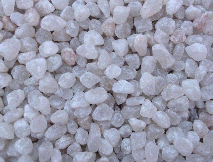
Chemical composition also plays a vital role. The quartz sand must consist predominantly of silicon dioxide (SiO2) with minimal trace elements that could affect the material's properties. A well-balanced chemical composition ensures that the fused silica exhibits the desired thermal, mechanical, and optical properties.
In summary, the careful selection of quartz sand based on these criteria is fundamental to producing high-quality fused silica, which is essential for its diverse and demanding applications across various industries.
Quartz Block Crushing and Powder Grinding
Quartz blocks undergo a meticulous process to transform into the fine powder necessary for producing high-quality fused silica. Initially, these blocks are subjected to crushing, which involves breaking them down into smaller, more manageable particles. This step is crucial as it sets the foundation for achieving the desired fineness in the subsequent grinding process.
The crushing process typically employs specialized equipment designed to handle the hardness and brittleness of quartz. These machines efficiently reduce the quartz blocks into granules, ensuring uniformity in size and minimizing the generation of unwanted by-products. The resultant granules are then transferred to grinding mills, where they are further processed to reach the required particle size.
Grinding is the final and most critical stage in this transformation. Advanced grinding techniques, often utilizing ball mills or jet mills, are employed to reduce the quartz particles to the sub-micron range. This level of fineness is essential for the subsequent melting process, as it ensures that the quartz powder can be uniformly heated and transformed into a homogeneous glass liquid.
The combination of crushing and grinding not only enhances the purity and homogeneity of the quartz powder but also significantly impacts the final properties of the fused silica. Achieving the desired fineness ensures that the resulting fused silica exhibits superior optical and mechanical properties, making it suitable for a wide range of high-tech applications.
Melting Process
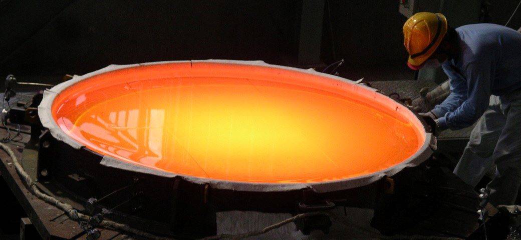
The transformation of fine quartz powder into fused silica begins with a meticulous melting process. This process involves the use of specialized high temperature furnace, which can reach temperatures exceeding 2,000°C. These furnaces are designed to ensure uniform heating, preventing any localized overheating that could compromise the purity of the final product.
Once the quartz powder reaches its melting point, it transitions into a viscous quartz glass liquid. This liquid state is crucial for achieving the homogeneity and high purity required for fused silica. The molten quartz is then carefully cooled and subjected to a controlled curing process. This cooling and curing phase is critical, as it determines the mechanical and optical properties of the resulting fused silica.
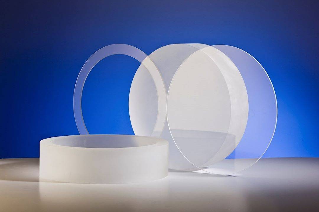
The entire process is meticulously monitored to ensure that the quartz glass liquid solidifies into a flawless, transparent material. This solidified form is what we recognize as fused silica, a material renowned for its exceptional properties that make it indispensable in various high-tech industries.
Applications of Fused Silica
Optical Device Manufacturing
Fused silica plays a pivotal role in the manufacturing of high-quality optical devices, including lenses, optical fibers, windows, and prisms. These components are integral to advanced technologies such as laser systems and optical communication networks. The unique optical properties of fused silica, such as its high transmittance and low optical absorption across a broad spectrum of wavelengths, make it an ideal material for these applications.
In laser technology, fused silica lenses and prisms are crucial for beam shaping and guiding, ensuring precise and efficient energy transfer. Similarly, in optical communications, fused silica optical fibers are used to transmit data over long distances with minimal loss, thanks to their exceptional transparency and mechanical strength.
| Application | Fused Silica Component | Benefit |
|---|---|---|
| Laser Technology | Lenses, Prisms | High transmittance, precise beam shaping |
| Optical Communications | Optical Fibers | Low signal loss, long-distance data transmission |
The use of fused silica in these applications underscores its importance in advancing modern optical technologies, enabling higher performance and reliability in critical systems.
Semiconductor Industry
Fused silica plays a pivotal role in the semiconductor industry, serving as a foundational material for the production of semiconductor devices and materials. Its unique properties make it indispensable in this high-tech sector. For instance, the high melting point of fused silica ensures that it can withstand the extreme temperatures required during semiconductor fabrication processes, such as photolithography and etching. This high thermal resistance is crucial for maintaining the structural integrity of the materials under intense heat conditions.
Moreover, the low thermal expansion coefficient of fused silica contributes to its stability and reliability in semiconductor manufacturing. This characteristic minimizes the risk of thermal stress-induced defects, which can compromise the performance and lifespan of semiconductor devices. Additionally, fused silica's chemical stability is vital for protecting semiconductor components from corrosive chemicals and contaminants that are commonly used in the fabrication process.
In summary, fused silica's combination of high melting point, low thermal expansion, and chemical stability makes it an essential material in the semiconductor industry, ensuring the production of high-quality, reliable semiconductor devices.
Chemical Industry and Photolithography
Fused silica's unique properties make it indispensable in both the chemical industry and photolithography. In the chemical sector, its exceptional corrosion resistance ensures that it can withstand harsh chemical environments, making it ideal for use in reactors, distillation columns, and other critical equipment. This durability not only extends the lifespan of the equipment but also reduces maintenance costs and downtime, contributing to more efficient and reliable chemical processes.
In the realm of photolithography, fused silica's high purity and optical transparency are leveraged to create masks and substrates for high-precision microelectronic manufacturing. The ability to maintain dimensional stability under extreme conditions is crucial for the fabrication of semiconductor devices, where even minute deviations can lead to significant defects. Fused silica's low thermal expansion coefficient further enhances its suitability for these applications, ensuring that the masks and substrates remain dimensionally consistent during the exposure and etching processes.
Moreover, the optical properties of fused silica, including its high transmittance across various wavelengths, make it an optimal choice for photolithography tools. This ensures that the light used in the photolithography process can accurately transfer intricate patterns onto the semiconductor wafers, enabling the production of smaller, more complex integrated circuits. As the semiconductor industry continues to push the boundaries of miniaturization and performance, the demand for high-quality fused silica in photolithography is expected to grow, driving advancements in microelectronic manufacturing technologies.
Market Prospects and Development Trends
Growth in Semiconductor and Optical Communication Markets
The demand for fused silica in the semiconductor and optical communication industries is poised for significant growth, driven by the relentless march of technological advancements and the burgeoning need for global connectivity. As the world becomes increasingly interconnected, the reliance on high-speed data transmission and sophisticated semiconductor devices has surged, creating a fertile ground for the expanded use of fused silica.
In the semiconductor industry, fused silica is indispensable due to its exceptional properties, including high purity, chemical stability, and thermal resistance. These characteristics make it ideal for the production of semiconductor devices, where even the slightest impurity can compromise performance. The growing complexity of semiconductor designs and the push towards smaller, more efficient chips further amplify the need for high-quality fused silica.
Similarly, the optical communication sector is witnessing unprecedented growth, fueled by the demand for faster and more reliable data transmission. Fused silica's superior optical properties, such as high transmittance across various wavelengths, make it a material of choice for optical fibers, lenses, and other critical components. The increasing deployment of 5G networks and the rise of the Internet of Things (IoT) are just a few examples of the technological advancements that are driving this demand.
To illustrate the magnitude of this growth, consider the following projections:
| Industry Segment | Current Annual Growth Rate | Expected Annual Growth Rate (2025) |
|---|---|---|
| Semiconductor | 5-7% | 8-10% |
| Optical Communication | 6-8% | 9-12% |
These figures underscore the promising outlook for fused silica, as both industries are set to expand at a rapid pace. The integration of artificial intelligence, autonomous vehicles, and advanced robotics will only serve to bolster this growth, ensuring that fused silica remains a cornerstone material in the future of technology.
Environmental Sustainability and Technological Innovation
The future trajectory of fused silica development is poised to be deeply intertwined with the principles of environmental sustainability and relentless technological innovation. As the global demand for high-performance materials continues to surge, the industry is under increasing pressure to adopt production methods that minimize environmental impact while maximizing efficiency and product quality.
One of the key areas of focus is the optimization of the production process to reduce energy consumption and emissions. This includes the exploration of renewable energy sources for powering high-temperature furnaces, which are critical in the melting process of fused silica. Additionally, advancements in recycling techniques are being developed to reclaim and reuse waste materials, thereby reducing the reliance on virgin raw materials.
Technological innovation is not limited to the production phase but extends to the enhancement of fused silica's intrinsic properties. Researchers are working on novel methods to improve its mechanical, thermal, and optical characteristics, making it even more suitable for a broader range of applications. For instance, nanotechnology is being leveraged to create fused silica with enhanced mechanical strength and reduced thermal expansion, which are crucial for high-precision applications in the semiconductor industry.
Moreover, the integration of smart manufacturing technologies, such as artificial intelligence and machine learning, is expected to revolutionize the production process. These technologies can optimize manufacturing parameters in real-time, ensuring consistent product quality and reducing waste. The adoption of Industry 4.0 principles will enable a more agile and responsive production system, capable of quickly adapting to market demands and regulatory changes.
In summary, the future of fused silica development will be characterized by a dual emphasis on environmental sustainability and technological innovation. By embracing these principles, the industry can not only meet the growing demand for high-performance materials but also contribute to a more sustainable and technologically advanced future.
International Market Competition and Diversified Demand
In the global market, fused silica producers face significant challenges from intensified international competition and the ever-evolving demands of various industries. This dynamic landscape necessitates continuous innovation and a relentless focus on enhancing product quality. The competitive pressures stem from both established players and emerging market entrants, each vying for a share in the lucrative fused silica market.

To maintain a competitive edge, producers must adopt a multifaceted approach. This includes investing in research and development to pioneer new production techniques and improve the overall performance of fused silica. For instance, advancements in melting processes can lead to higher purity levels, which are crucial for applications in the semiconductor and optical industries. Additionally, producers need to stay attuned to the specific requirements of different sectors, such as the need for higher thermal stability in aerospace applications or superior optical properties in medical devices.
Moreover, the diversification of demand across various industries underscores the importance of flexibility in production capabilities. Producers must be capable of tailoring their products to meet the unique specifications of each market segment. This adaptability not only helps in securing current contracts but also positions the company favorably for future opportunities. For example, the growing emphasis on environmental sustainability could drive demand for fused silica with reduced carbon footprints, encouraging producers to explore eco-friendly production methods.
In summary, the combination of fierce international competition and diversified market demands compels fused silica producers to innovate continuously. By focusing on quality improvement, technological advancements, and market-specific adaptations, these producers can ensure their sustained competitiveness in the global fused silica market.