Introduction to Glass Substrates in Semiconductor Packaging
Intel's Announcement and Industry Response
Since September 2023, Intel has set the semiconductor industry abuzz with its ambitious plan to introduce a glass substrate for next-generation advanced packaging by 2030. This groundbreaking announcement has prompted major packaging and testing companies to initiate strategic planning for the adoption of glass substrates. The impetus behind this transformative move is the escalating demand for high-performance chips, particularly in AI and GPU applications, where the need for superior thermal management and electrical performance is paramount.
The industry's response to Intel's announcement has been swift and strategic. Key players are aligning their R&D efforts to explore the potential of glass substrates, recognizing the significant advantages they offer over traditional materials. Glass substrates, with their superior thermal conductivity and mechanical stability, are seen as a game-changer in the quest for more efficient and powerful semiconductor solutions.
Moreover, the shift towards glass substrates is not merely reactive but proactive, driven by the evolving landscape of semiconductor technology. As AI and GPU applications continue to push the boundaries of computational power, the industry is compelled to innovate and adopt materials that can sustain and enhance these capabilities. Intel's foresight in this domain has thus catalyzed a wave of strategic initiatives across the sector, setting the stage for what could be a paradigm shift in semiconductor packaging.
Role and Importance of Substrates in Electronics
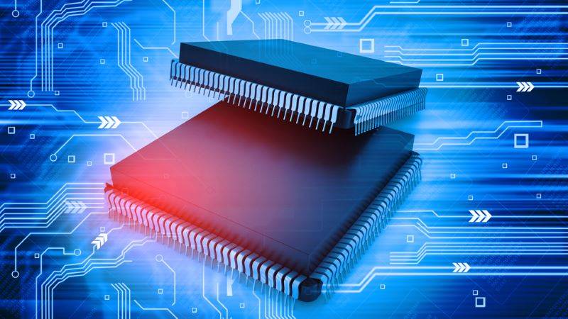
Substrates play a pivotal role in the realm of electronics, particularly within the context of printed circuit boards (PCBs) and semiconductor components. As essential carriers and connectors, they provide a robust foundation that ensures the stability, insulation, and thermal management necessary for the optimal performance and longevity of electronic components.
In the intricate architecture of modern electronics, substrates act as the backbone, supporting and interconnecting various elements. They offer mechanical stability, which is crucial for maintaining the integrity of delicate electronic components during operation and transportation. This stability is particularly vital in high-frequency and high-speed applications, where even minor displacements can lead to significant performance degradation.
Moreover, substrates are designed to insulate different layers of circuitry, preventing short circuits and ensuring the efficient operation of electronic devices. This insulation is achieved through the use of materials with low dielectric constants, which minimize signal loss and interference, thereby enhancing the overall efficiency and reliability of the device.
Thermal management is another critical function of substrates. As electronic components generate heat during operation, substrates must facilitate effective heat dissipation to prevent overheating, which can lead to performance issues or even component failure. Advanced substrates often incorporate thermal vias and materials with high thermal conductivity to efficiently transfer heat away from sensitive areas, ensuring consistent performance and extending the lifespan of the device.
In summary, substrates are indispensable in the electronics industry, serving as the linchpin that holds together the various components of a device. Their ability to provide stability, insulation, and thermal management makes them essential for the reliable and efficient operation of electronic systems, from simple consumer gadgets to complex high-performance computing chips.
Specialty Substrates and Their Evolution
BT Resin Substrate
BT resin, a sophisticated blend of bismaleimide resin and cyanate ester resin, stands out in the semiconductor industry for its exceptional thermal and mechanical properties. This unique combination endows BT resin with high heat resistance, a low dielectric constant, and superior mechanical strength, making it an ideal choice for a variety of advanced applications.
BT resin substrates are particularly renowned for their dimensional stability and reliability, which are critical factors in the performance of electronic components. These properties have made BT resin substrates a preferred choice for memory chips, Micro-Electro-Mechanical Systems (MEMS), Radio Frequency (RF) chips, and Light Emitting Diode (LED) chips. The dimensional stability ensures that the substrate maintains its form under varying thermal conditions, while the reliability ensures long-term performance and durability.

In addition to its thermal and mechanical advantages, BT resin substrates offer excellent electrical insulation, which is essential for preventing signal interference and ensuring the integrity of data transmission. This combination of properties positions BT resin substrates as a cornerstone in the development of high-performance electronic devices, particularly in applications where heat dissipation and mechanical robustness are paramount.
The widespread adoption of BT resin substrates in these critical areas underscores its importance in advancing semiconductor technology, particularly as the industry continues to push the boundaries of what is possible in miniaturization and performance.
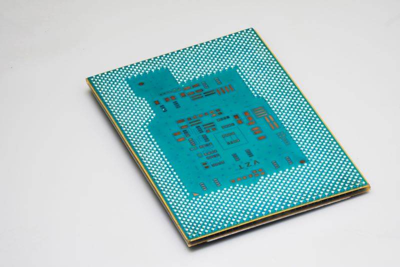
ABF Resin Substrates
Developed by Ajinomoto, ABF resin substrates are renowned for their exceptional properties that make them ideal for high-performance computing applications. These substrates boast high density, rigidity, and durability, which are critical attributes for supporting the demanding requirements of chips used in CPUs, GPUs, and FPGAs. The high-density interconnectivity facilitated by ABF resin substrates enables more efficient data processing and faster computational speeds.
However, the reliability of ABF resin substrates is compromised by thermal expansion issues. As these substrates are subjected to varying temperatures, their dimensional stability can be affected, leading to potential misalignment of components and reduced overall performance. This thermal expansion challenge necessitates ongoing research and development to enhance the material's thermal stability, ensuring consistent performance under diverse operational conditions.
To address these challenges, several strategies are being explored. One approach involves modifying the resin composition to improve thermal resistance and reduce expansion coefficients. Additionally, advancements in manufacturing processes are being pursued to better control the substrate's dimensional consistency during production. These efforts aim to mitigate the negative impacts of thermal expansion, thereby enhancing the long-term reliability and performance of ABF resin substrates in high-performance computing environments.
Advantages and Challenges of Glass Substrates
Key Benefits of Glass Substrates
Glass substrates stand out due to their exceptional thermal conductivity, optical transparency, and mechanical stability, which collectively make them an ideal choice for high-performance semiconductor chips. These properties are particularly advantageous in the context of advanced semiconductor packaging, where heat dissipation, optical performance, and interconnection density are critical factors.
Enhanced Heat Dissipation
One of the most significant benefits of glass substrates is their ability to significantly enhance heat dissipation. Unlike traditional substrates that can trap heat, glass substrates facilitate efficient heat transfer, ensuring that the chips operate at optimal temperatures. This is crucial for maintaining the performance and longevity of high-performance chips, especially in applications like artificial intelligence (AI) and graphics processing units (GPUs) where heat generation is substantial.
Optical Performance
Glass substrates offer unparalleled optical transparency, which is essential for applications requiring precise optical alignment and signal transmission. This transparency allows for better light transmission and reduced signal loss, enhancing the overall optical performance of the semiconductor devices. This feature is particularly beneficial in high-speed data transmission and optical communication systems.
Improved Interconnection Density
Another key advantage of glass substrates is their ability to support higher interconnection density. The mechanical stability of glass allows for more precise and compact interconnections, which is vital for the miniaturization of semiconductor devices. This increased density translates to faster computation and improved energy efficiency, making glass substrates a preferred choice for next-generation semiconductor packaging.
Summary of Benefits
| Benefit | Description |
|---|---|
| Heat Dissipation | Efficient heat transfer ensures optimal chip performance and longevity. |
| Optical Performance | Unmatched optical transparency for better signal transmission and alignment. |
| Interconnection Density | Supports higher density for faster computation and energy efficiency. |
In summary, the combination of superior thermal conductivity, optical transparency, and mechanical stability positions glass substrates as a transformative material in the realm of advanced semiconductor packaging, promising significant advancements in chip performance and efficiency.

Technical Challenges and Proposed Solutions
Glass substrates, while offering significant advantages such as high thermal conductivity and optical transparency, are not without their challenges. One of the primary issues is their inherent fragility, which can lead to breakage during handling and manufacturing processes. Additionally, the technology for perforating glass substrates is still in its infancy, making it difficult to achieve the precise, high-density perforations required for advanced semiconductor applications.
Thermal stress warpage is another critical concern, as the thermal expansion properties of glass can cause significant deformation under high temperatures, affecting the substrate's flatness and, consequently, the performance of the integrated circuits. To address these challenges, several proposed solutions are being explored.
One approach involves modifying the composition of the glass to enhance its mechanical properties. By introducing additives that improve toughness and reduce brittleness, it is possible to create a more durable glass substrate that can withstand the rigors of semiconductor manufacturing. Additionally, new manufacturing processes are being developed to improve perforation technology, ensuring that holes can be drilled with high precision and minimal damage to the surrounding material.
Another promising solution is the adjustment of substrate thickness. By optimizing the thickness of the glass substrate, it is possible to mitigate warpage caused by thermal stress. Thicker substrates can better distribute thermal loads, reducing the likelihood of deformation. Conversely, thinner substrates can be designed with specific reinforcement structures to maintain flatness under thermal stress.
These proposed solutions are not only aimed at overcoming the current limitations of glass substrates but also at paving the way for their widespread adoption in advanced semiconductor packaging. As the industry continues to innovate, the goal is to create glass substrates that combine the benefits of high performance with the robustness necessary for industrial-scale production.
Industry Trends and Future Outlook
Intel's Vision and Industry Adoption
Intel, alongside industry giants such as Samsung, Apple, and Lehman Optoelectronics, is spearheading the investment in glass substrate technology. This collective effort underscores a shared vision for the future of semiconductor packaging, where glass substrates are poised to become the dominant material. The industry's optimism is fueled by ongoing advancements that are expected to overcome the current limitations associated with glass substrates.
These companies recognize the transformative potential of glass substrates in enhancing thermal conductivity, optical transparency, and mechanical stability—key attributes that are critical for high-performance chips. By investing heavily in research and development, they aim to address challenges such as fragility, perforation technology, and thermal stress warpage. Proposed solutions include refining glass compositions, innovating manufacturing processes, and optimizing substrate thickness to mitigate warpage.
The strategic investments and collaborative efforts within the industry are not just about overcoming technical hurdles; they are also about positioning themselves to capitalize on the growing demand for high-performance chips in AI and GPU applications. As Intel's announcement in September 2023 indicated, the transition to glass substrates is seen as a necessary step to meet the escalating requirements of next-generation advanced packaging by 2030.
In summary, the concerted efforts by Intel and other major tech players are laying the groundwork for glass substrates to revolutionize semiconductor packaging. The industry's confidence in this technology's future is a testament to the significant strides being made to ensure that glass substrates can effectively meet the demands of the rapidly evolving semiconductor landscape.
Related Products
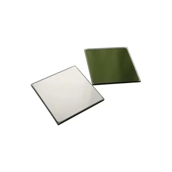
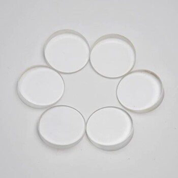
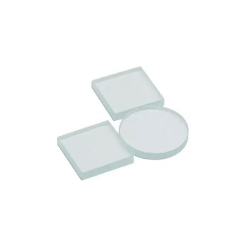
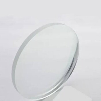
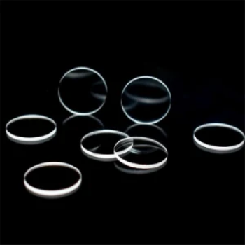
- Optical Window Glass Substrate Wafer Single Double Sided Coated K9 Quartz Sheet
- Optical Window Glass Substrate Wafer Quartz Plate JGS1 JGS2 JGS3
- Optical Window Glass Substrate Wafer CaF2 Substrate Window Lens
- Float Soda-Lime Optical Glass for Laboratory Use
- Custom PTFE Teflon Parts Manufacturer for Conductive Glass Substrate Cleaning Rack
Related Articles
- The Fidelity of Light: Preserving the Quartz Interface in Spectroelectrochemistry
- Factors in Selecting Large Optical Windows
- The Architecture of Silence: Why Material Choice Defines Electrochemical Truth
- Optical Components: Window Sheets and Their Applications
- Comprehensive Guide to Optical Windows: Material Properties and Surface Specifications