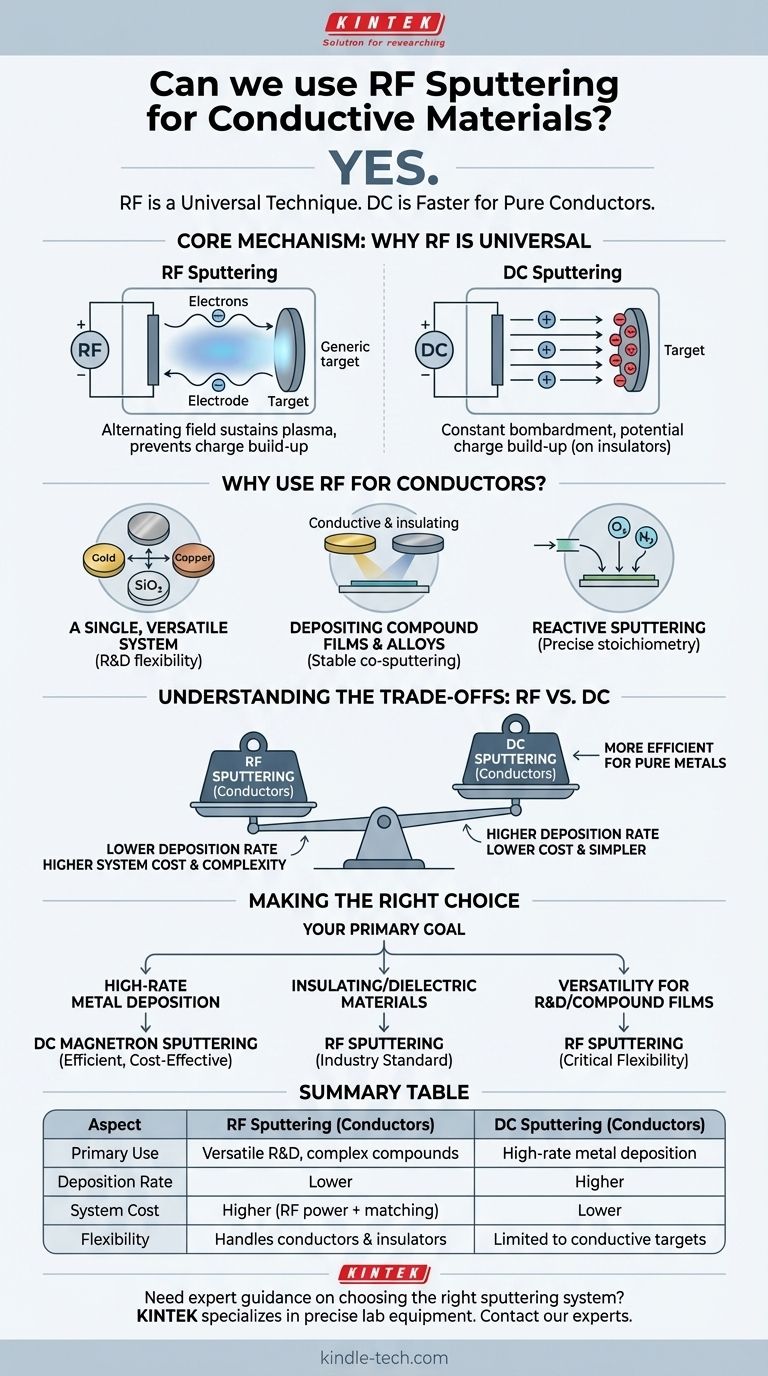
Yes, you can absolutely use RF sputtering for conductive materials. While Radio Frequency (RF) sputtering is renowned for its unique ability to deposit insulating materials, it is a highly versatile technique that works perfectly well for depositing metals, alloys, and other conductors. Its mechanism for generating plasma is material-agnostic, making it a universal sputtering method.
The central takeaway is that RF sputtering is a "do-it-all" deposition technique. However, for purely conductive targets, traditional DC sputtering is often faster and more cost-effective. The choice between RF and DC depends on whether you need maximum versatility for all material types or maximum efficiency for conductors alone.
The Core Mechanism: Why RF Sputtering is Universal
Sustaining Plasma with an Alternating Field
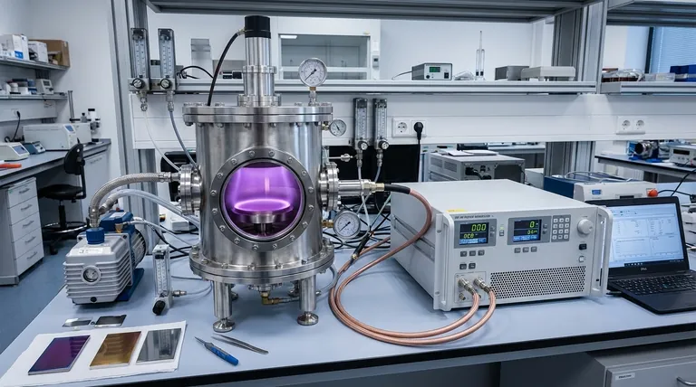
The defining feature of RF sputtering is its use of a high-frequency alternating current power source. This rapidly switching electric field continuously accelerates electrons back and forth within the process chamber.
These oscillating electrons collide with neutral gas atoms (typically Argon), knocking off other electrons and creating a stable, self-sustaining plasma. The positive ions from this plasma are then accelerated toward the target material, bombarding it and ejecting atoms that deposit onto your substrate.
Bypassing the "Charge Build-up" Problem
The primary advantage of the RF method, and the reason it's essential for insulators, is that it prevents charge build-up. In DC sputtering, positive ions continuously bombard the target. If the target is an insulator, it cannot dissipate this positive charge, which eventually repels incoming ions and shuts down the sputtering process.
The alternating field of RF sputtering effectively neutralizes this charge build-up on the target surface during each cycle, allowing for the continuous, stable sputtering of non-conductive materials.
RF for Conductors: When and Why?
While a DC power supply is sufficient to sputter a conductive target, there are specific scenarios where using an RF source is practical and even advantageous.
A Single, Versatile System
For research and development labs, flexibility is key. An RF sputtering system can deposit virtually any material, from pure metals like gold and copper to complex dielectric compounds like silicon dioxide (SiO2).
Having a single RF system eliminates the need for separate DC power supplies, simplifying the equipment setup and allowing operators to switch between depositing conductors and insulators seamlessly.
Depositing Compound Films and Alloys
RF sputtering excels in more complex deposition processes. When co-sputtering from multiple targets—for instance, one conductive and one insulating—an RF power source provides a stable and reliable plasma environment for both.
It is also ideal for reactive sputtering, where a reactive gas is introduced to form a compound film on the substrate. The stable plasma control offered by RF systems is beneficial for achieving precise stoichiometry in the final film.
Understanding the Trade-offs: RF vs. DC for Conductors
Using RF sputtering for conductive materials is perfectly viable, but it comes with trade-offs compared to the more traditional DC sputtering method.
Deposition Rate and Efficiency
For a simple conductive target, DC magnetron sputtering is generally more efficient and achieves a higher deposition rate. The power is transferred directly and continuously to the target, leading to a more energetic and efficient sputtering process.
RF systems, due to their complexity and the nature of the power delivery, often result in lower deposition rates for the same input power when sputtering pure metals.
System Complexity and Cost
RF sputtering systems are inherently more complex and expensive. They require a dedicated RF power supply and an impedance matching network to efficiently transfer power to the plasma.
In contrast, DC power supplies are simpler, more robust, and significantly less expensive. For high-volume industrial applications focused solely on depositing metals, DC sputtering is almost always the more economical choice.
Making the Right Choice for Your Goal
To select the appropriate technique, you must align the method's strengths with your primary objective.
- If your primary focus is high-rate deposition of pure metals: DC magnetron sputtering is the more efficient and cost-effective choice.
- If your primary focus is depositing insulating or dielectric materials: RF sputtering is the necessary and standard industry method.
- If your primary focus is versatility for R&D or complex compound films: An RF sputtering system provides the critical flexibility to handle any material you need.
Ultimately, your choice is a strategic decision between specialization and versatility.
Summary Table:
| Aspect | RF Sputtering (for Conductors) | DC Sputtering (for Conductors) |
|---|---|---|
| Primary Use | Versatile R&D, complex compounds | High-rate metal deposition |
| Deposition Rate | Lower | Higher |
| System Cost | Higher (RF power supply + matching network) | Lower |
| Flexibility | Handles conductors & insulators | Limited to conductive targets |
Need expert guidance on choosing the right sputtering system for your lab?
At KINTEK, we specialize in providing precise lab equipment and consumables for all your deposition needs. Whether you require the versatility of an RF system for R&D or the high efficiency of a DC setup for production, our experts will help you optimize your thin film processes.
Contact our team today to discuss your specific application and get a tailored solution that maximizes your lab's performance and ROI.
Visual Guide
Related Products
- RF PECVD System Radio Frequency Plasma-Enhanced Chemical Vapor Deposition RF PECVD
- Horizontal High Temperature Graphite Vacuum Graphitization Furnace
- Spark Plasma Sintering Furnace SPS Furnace
- Automatic Laboratory Hydraulic Press for XRF & KBR Pellet Press
- Electron Beam Evaporation Coating Oxygen-Free Copper Crucible and Evaporation Boat
People Also Ask
- How does Radio Frequency Enhanced Plasma Chemical Vapour Deposition (RF-PECVD) work? Learn the Core Principles
- What is plasma CVD? Unlock Low-Temperature Thin Film Deposition for Sensitive Materials
- What is plasma enhanced chemical vapour deposition process? Unlock Low-Temperature, High-Quality Thin Films
- What is an example of PECVD? RF-PECVD for High-Quality Thin Film Deposition
- What is the role of RF-PECVD in VFG preparation? Mastering Vertical Growth and Surface Functionality


