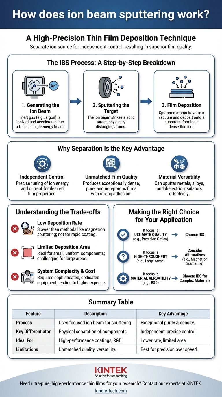
At its core, ion beam sputtering (IBS) is a high-precision thin film deposition technique. It uses a focused, high-energy beam of ions to physically dislodge atoms from a source material, known as the "target." These dislodged atoms then travel through a high-vacuum chamber and deposit onto a component, or "substrate," forming an exceptionally dense and high-quality film.
Unlike other methods where plasma is in direct contact with both the target and the substrate, ion beam sputtering separates the ion source from the target. This decoupling provides independent, precise control over the deposition process, resulting in films with superior density, purity, and performance.
The IBS Process: A Step-by-Step Breakdown
The effectiveness of ion beam sputtering comes from its methodical and highly controlled nature. The entire process takes place inside a high-vacuum chamber to ensure the purity of the final film.
Step 1: Generating the Ion Beam
The process begins with an ion source, which is a distinct module separate from the material being deposited. An inert gas, typically argon, is fed into this source. Energy is applied to strip electrons from the argon atoms, creating a plasma of positively charged argon ions.
These ions are then extracted and accelerated by an electric field, forming a well-defined, high-energy ion beam.
Step 2: Sputtering the Target
This collimated (parallel) and monoenergetic (uniform energy) beam of ions is directed at the target. The target is a solid block of the material you wish to deposit, such as a metal or dielectric.
When the high-energy ions strike the target, they transfer their momentum to the atoms on the target's surface. If the energy transfer is sufficient, it knocks atoms loose from the target material in a process known as sputtering.
Step 3: Film Deposition
The sputtered atoms travel in a straight line through the vacuum until they strike the substrate. Upon arrival, they condense on the substrate's surface, gradually building a thin film one atomic layer at a time.
Because this process occurs in a clean, low-pressure environment without the chaotic plasma of other methods, the resulting film is extremely pure and dense.
Why Separation is the Key Advantage
The defining characteristic of IBS is the physical separation between the ion source, the target, and the substrate. This architecture is the source of its primary benefits.
Independent Control
Because the ion source is independent, operators can precisely tune the ion beam's energy and current (the number of ions per second). This allows for fine-tuning the deposition rate and the energy of the depositing atoms, which directly impacts the final film's properties.
Unmatched Film Quality
The controlled, monoenergetic ion beam produces films with superior characteristics. The films are exceptionally dense, non-porous, and have a strong bond to the substrate. This quality is critical for demanding applications like precision optics.
Material Versatility
Since the target is not part of the electrical circuit creating the ions, IBS can effectively sputter nearly any material. This includes metals, alloys, and dielectric insulators, making it a highly versatile tool for both production and research.
Understanding the Trade-offs
While powerful, IBS is not the right solution for every application. Its precision comes with clear limitations that must be considered.
Low Deposition Rate
IBS is a deliberate and relatively slow process. The rate at which material is sputtered and deposited is significantly lower than higher-volume methods like magnetron sputtering. This makes it less suitable for applications requiring rapid coating.
Limited Deposition Area
The focused nature of the ion beam makes it ideal for coating smaller components with high uniformity. However, achieving this same uniformity over large surface areas is a significant challenge and often impractical with standard IBS systems.
System Complexity and Cost
The need for a dedicated ion source, sophisticated high-vacuum chambers, and precise control systems makes IBS equipment more complex and expensive than simpler deposition technologies.
Making the Right Choice for Your Application
Deciding if IBS is the correct method requires weighing its precision against its inherent speed and scale limitations. Use the following guide to make an informed choice.
- If your primary focus is ultimate film quality and precision: IBS is the superior choice for applications like high-performance optical coatings or advanced semiconductor layers where material properties are paramount.
- If your primary focus is high-throughput or coating large areas: You should consider alternative methods like magnetron sputtering, which offer much higher deposition rates at the cost of some film quality and control.
- If your primary focus is material versatility for complex research: The ability of IBS to cleanly sputter insulators and complex alloys makes it an invaluable tool for materials science and R&D.
Ultimately, ion beam sputtering is the definitive tool when the performance and quality of the thin film cannot be compromised.
Summary Table:
| Feature | Description | Key Advantage |
|---|---|---|
| Process | Uses a focused ion beam to sputter atoms from a target in a high-vacuum chamber. | Exceptional film purity and density. |
| Key Differentiator | Physical separation of the ion source, target, and substrate. | Independent, precise control over deposition parameters. |
| Ideal For | High-performance optical coatings, semiconductor layers, and complex material R&D. | Unmatched film quality and material versatility. |
| Limitations | Lower deposition rate and limited area coverage compared to other methods. | Best suited for precision applications over high throughput. |
Need to deposit ultra-pure, high-performance thin films for your research or production?
KINTEK specializes in providing advanced lab equipment and consumables for demanding laboratory needs. Our expertise in deposition technologies like ion beam sputtering can help you achieve the precise, high-quality coatings your work requires.
Contact our experts today to discuss how our solutions can enhance your lab's capabilities and drive your projects forward.
Visual Guide
Related Products
- Electron Beam Evaporation Coating Gold Plating Tungsten Molybdenum Crucible for Evaporation
- Electron Beam Evaporation Coating Oxygen-Free Copper Crucible and Evaporation Boat
- E Beam Crucibles Electron Gun Beam Crucible for Evaporation
- Electron Beam Evaporation Coating Conductive Boron Nitride Crucible BN Crucible
People Also Ask
- What is the process of e-beam coating? Achieve High-Purity, Precise Thin Films for Your Lab
- What is e-beam evaporation used for? Precision Coating for Optics, Aerospace & Electronics
- What materials are used in electron beam evaporation? Master High-Purity Thin Film Deposition
- What is the voltage of e-beam evaporation? Achieve Precise Thin-Film Deposition
- How is an electron beam evaporator cooled during deposition? Essential Thermal Management for Stable Processes


