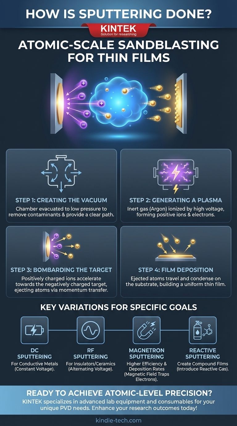
At its core, sputtering is a physical process used to create ultra-thin films of material with atomic-level precision. It involves ejecting atoms from a source material, called a "target," by bombarding it with energetic ions inside a vacuum. These ejected atoms then travel and condense onto a surface, known as a "substrate," forming a new, highly uniform layer.
The most effective way to understand sputtering is to visualize it as a form of atomic-scale sandblasting. Instead of using sand to strip a surface, you use a super-charged gas (plasma) to knock individual atoms off a source material, which then rebuild a new surface atom by atom on a different object.
The Core Principle: Controlled Atomic Collision
Sputtering is a type of Physical Vapor Deposition (PVD). Unlike processes that evaporate material with heat, sputtering uses pure momentum transfer to liberate atoms. This gives it exceptional control over the film's properties. The entire process unfolds in a series of carefully controlled steps inside a vacuum chamber.
Step 1: Creating a Controlled Environment (The Vacuum)
Before the process can begin, the chamber is sealed and evacuated to an extremely low pressure.
This vacuum is critical for two reasons. First, it removes contaminants like air and water vapor that would otherwise get embedded in the film and compromise its purity. Second, it provides a clear, obstacle-free path for the sputtered atoms to travel from the target to the substrate.
Step 2: Generating a Plasma (The "Sandblaster")
Once the vacuum is established, a small, precisely controlled amount of an inert gas, almost always Argon (Ar), is introduced into the chamber.
A high voltage is then applied. This electrical energy strips electrons from the argon atoms, creating a glowing, ionized gas known as a plasma. This plasma is a "soup" of positively charged argon ions (Ar+) and free electrons.
Step 3: Bombarding the Target (The Impact)
The source material, or target, is given a strong negative electrical charge.
Just as opposite poles of a magnet attract, the positively charged argon ions in the plasma are forcefully accelerated toward the negatively charged target. They collide with the target's surface with tremendous kinetic energy.
This impact is the "sputtering" event. The energy from the ion collision is transferred to the atoms in the target, giving them enough energy to be knocked loose, or ejected, from the surface.
Step 4: Transport and Deposition (Building the Film)
The ejected atoms from the target are neutral particles. They are not affected by the electric fields in the chamber.
These atoms travel in a straight line through the vacuum until they strike a surface. By strategically placing your object (the substrate) in front of the target, you ensure these traveling atoms land on it.
As they arrive, the atoms condense on the substrate's surface, gradually building up a thin, dense, and highly uniform film.
Understanding the Trade-offs and Variations
While the core principle is the same, several sputtering techniques exist, each optimized for different materials and outcomes. Understanding these is key to leveraging the process effectively.
DC vs. RF Sputtering: The Role of Material Conductivity
The simplest method, DC (Direct Current) sputtering, uses a constant negative voltage. This works perfectly for electrically conductive targets, like most metals.
However, if the target is an electrical insulator (like a ceramic), a positive charge will quickly build up on its surface, repelling the incoming argon ions and stopping the process. For these materials, RF (Radio Frequency) sputtering is used. It rapidly alternates the voltage, preventing charge buildup and allowing insulating materials to be sputtered.
Magnetron Sputtering: Enhancing Efficiency
Modern sputtering systems almost always incorporate magnets behind the target. This technique is called magnetron sputtering.
The magnetic field traps the free electrons from the plasma near the target's surface. These trapped electrons travel in a spiral path, dramatically increasing their chances of colliding with and ionizing more argon atoms. This creates a much denser, more intense plasma right where it's needed, leading to higher deposition rates and allowing the process to run at lower pressures.
Reactive Sputtering: Creating Compounds
While argon is used because it is inert, you can intentionally introduce a reactive gas like oxygen or nitrogen along with it.
In this process, known as reactive sputtering, the sputtered metal atoms react with the gas on their way to the substrate. This allows you to deposit compound films, such as titanium nitride (a hard coating) or silicon dioxide (an optical coating), directly onto the substrate.
Making the Right Choice for Your Goal
The specific sputtering method you choose depends entirely on the material you wish to deposit and the properties you need the final film to have.
- If your primary focus is a simple metallic film: Standard DC magnetron sputtering is the most efficient and widely used method.
- If your primary focus is a ceramic or insulating film: RF magnetron sputtering is essential to handle the non-conductive target material.
- If your primary focus is a compound film (like an oxide or nitride): Reactive sputtering is the correct technique to form the desired chemical compound during deposition.
Ultimately, sputtering's power lies in its precise, repeatable control over the creation of new surfaces.
Summary Table:
| Sputtering Step | Key Action | Purpose |
|---|---|---|
| 1. Vacuum Creation | Evacuate chamber to low pressure | Remove contaminants, provide clear atom path |
| 2. Plasma Generation | Introduce argon gas, apply high voltage | Create ionized gas (Ar+ ions) for bombardment |
| 3. Target Bombardment | Accelerate ions toward negatively charged target | Eject atoms from source material via momentum transfer |
| 4. Film Deposition | Ejected atoms travel and condense on substrate | Build uniform, high-purity thin film layer |
| Key Variations | DC Sputtering (metals), RF Sputtering (insulators), Magnetron (higher efficiency), Reactive (compound films) | Tailor process for specific material and coating requirements |
Ready to achieve atomic-level precision in your thin film applications?
KINTEK specializes in advanced lab equipment and consumables for sputtering and other Physical Vapor Deposition (PVD) processes. Whether you're working with conductive metals, insulating ceramics, or need to create custom compound films, our expertise ensures you get the right solution for your laboratory's unique needs.
Contact us today to discuss how our sputtering systems and support can enhance your research and development outcomes.
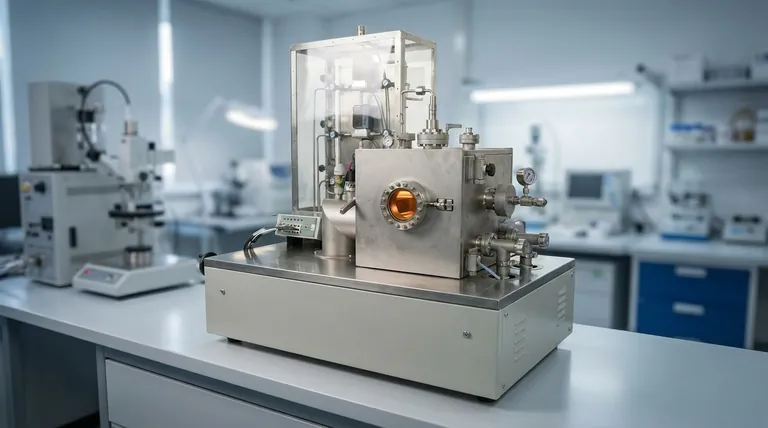
Visual Guide
Related Products
- Spark Plasma Sintering Furnace SPS Furnace
- Vacuum Induction Melting Spinning System Arc Melting Furnace
- Chemical Vapor Deposition CVD Equipment System Chamber Slide PECVD Tube Furnace with Liquid Gasifier PECVD Machine
- Customer Made Versatile CVD Tube Furnace Chemical Vapor Deposition Chamber System Equipment
People Also Ask
- What is the theory of spark plasma sintering? A Guide to Rapid, Low-Temperature Densification
- What is the difference between spark plasma sintering and flash sintering? A Guide to Advanced Sintering Methods
- What is SPS sintering method? A Guide to High-Speed, High-Performance Material Fabrication
- What is the process fundamentals of spark plasma sintering? Achieve Rapid, High-Density Material Consolidation
- What are the fundamentals of spark plasma sintering process? Unlock Rapid, High-Performance Material Consolidation


