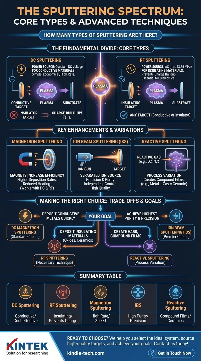
While many names exist, the field of physical vapor deposition is primarily built upon two fundamental types of sputtering: DC Sputtering and RF Sputtering. The core difference lies in the power source used to generate the plasma, which directly dictates the types of materials you can deposit. All other variations are essentially enhancements or specialized applications of these two core techniques.
The choice of a sputtering method is not arbitrary; it is a direct consequence of the material you need to deposit. Your decision boils down to matching the electrical properties of your target material—whether it is a conductor or an insulator—to the correct sputtering technique.
The Fundamental Divide: DC vs. RF Sputtering
At the heart of any sputtering process is a plasma—an ionized gas (typically argon) that provides the ions needed to bombard a target. The method used to create and sustain this plasma is the primary point of classification.
DC Sputtering: The Workhorse for Conductors
Direct Current (DC) sputtering is the simplest form. A high negative DC voltage is applied to the target material, which acts as a cathode. This ignites a plasma, and the positively charged argon ions are accelerated directly toward the negative target, dislodging atoms upon impact.
Because this method relies on a constant DC voltage, the target material must be electrically conductive. If the target were an insulator, positive charge would quickly accumulate on its surface, neutralizing the negative potential and halting the sputtering process.
RF Sputtering: The Solution for Insulators
Radio Frequency (RF) sputtering uses a high-frequency alternating current (AC) power source, typically at 13.56 MHz. This rapidly alternating electric field energizes electrons in the plasma, which then collide with and ionize the argon atoms.
The key advantage is that the alternating field prevents charge from building up on the surface of an insulating target. During one half of the cycle, the surface is bombarded by ions; during the other, it is neutralized by electrons. This versatility makes RF sputtering essential for depositing dielectric and ceramic materials.
Key Enhancements and Variations
Building on the DC and RF foundations, engineers have developed several advanced techniques to improve efficiency, deposition rates, and film quality.
Magnetron Sputtering: Increasing Speed and Efficiency
This is the most common enhancement used in modern systems. Magnets are placed behind the target to create a magnetic field that traps electrons in a path close to the target surface.
This trapping dramatically increases the probability of electrons colliding with and ionizing argon atoms, creating a much denser plasma. The result is a significantly higher deposition rate and reduced substrate heating. Both DC and RF systems are commonly upgraded to become DC Magnetron or RF Magnetron sputtering systems.
Ion Beam Sputtering (IBS): Precision and Purity
In ion beam sputtering, the plasma generation is physically separated from the target. An independent ion source, or "gun," generates a focused beam of ions that is aimed at the target material.
This separation gives independent control over ion energy and flux, allowing for extremely precise and repeatable deposition. IBS produces very dense, pure, and high-quality films, making it ideal for demanding applications like precision optics.
Reactive Sputtering: Creating Compound Films
Reactive sputtering is not a distinct type of system but rather a process variation. It involves introducing a reactive gas, such as oxygen or nitrogen, into the vacuum chamber along with the inert sputtering gas (argon).
The sputtered metal atoms travel from the target and react with this gas either in flight or on the substrate surface. This process is used to deposit compound films like titanium nitride (TiN) or aluminum oxide (Al₂O₃) from a pure metal target.
Understanding the Trade-offs
Choosing a sputtering technique involves balancing performance, complexity, and cost. Each method comes with inherent advantages and disadvantages.
Deposition Rate vs. Film Quality
Magnetron sputtering offers the highest deposition rates, making it ideal for industrial-scale production. However, methods like Ion Beam Sputtering, while much slower, provide superior control over film properties, resulting in higher density and purity.
System Complexity vs. Capability
A simple DC diode system is the least complex and cheapest to build. Adding RF capabilities or a magnetron array increases complexity and cost but dramatically expands the range of materials and improves efficiency. Ion Beam systems are the most complex and expensive, reserved for applications where ultimate film quality is non-negotiable.
Material Limitations
This is the most critical trade-off. If you must deposit an insulating material, you have no choice but to use an RF-based system. For simple metallic coatings, a DC magnetron system is almost always the most economical and efficient solution.
Making the Right Choice for Your Goal
Your application's specific requirements will guide your selection of the appropriate sputtering technique.
- If your primary focus is depositing conductive metals quickly and cost-effectively: DC Magnetron Sputtering is the standard industrial choice.
- If your primary focus is depositing insulating materials like oxides or ceramics: RF Sputtering (typically RF Magnetron) is the necessary technique.
- If your primary focus is creating hard, ceramic-like compound films from a metal target: Reactive Sputtering is the process you need to use.
- If your primary focus is achieving the highest possible film purity, density, and uniformity: Ion Beam Sputtering is the premier choice, despite its lower speed and higher cost.
Understanding these core methods transforms sputtering from a list of terms into a powerful toolkit for precision engineering.
Summary Table:
| Method | Best For | Key Advantage |
|---|---|---|
| DC Sputtering | Conductive Materials | Simple, Cost-Effective |
| RF Sputtering | Insulating Materials | Prevents Charge Buildup |
| Magnetron Sputtering | High Deposition Rates | Increased Efficiency & Speed |
| Ion Beam Sputtering (IBS) | High-Purity Films | Superior Control & Precision |
| Reactive Sputtering | Compound Films (e.g., TiN) | Creates Ceramics from Metals |
Ready to Choose the Right Sputtering Technique?
Navigating the different types of sputtering can be complex, but you don't have to do it alone. KINTEK specializes in lab equipment and consumables, providing expert solutions for all your deposition needs.
We can help you:
- Select the ideal system (DC, RF, Magnetron) for your specific materials and applications.
- Source high-quality targets and consumables to ensure optimal performance.
- Achieve your research and production goals with reliable, precision equipment.
Contact us today to discuss your project and let our experts guide you to the perfect sputtering solution.
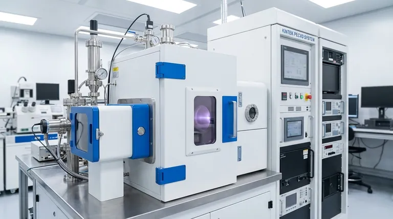
Visual Guide
Related Products
- Lab Sterile Slapping Type Homogenizer for Tissue Mashing and Dispersing
- Spark Plasma Sintering Furnace SPS Furnace
- Single Punch Manual Tablet Press Machine TDP Tablet Punching Machine
People Also Ask
- How do lab stirrers & homogenizers ensure uniform distribution? Optimize Your Complex Multiphase Chemical Mixing
- What role does a laboratory homogenizer play in radioactive cesium detection? Ensure Accuracy in Wildlife Sampling
- What role does an ultrasonic cleaner play in the pre-treatment of 4140 steel? Ensure Uniform Nitriding Activation
- Why is it necessary to use an ultrasonic cell disruptor before yeast flow cytometry? Ensure Data Accuracy
- What is the role of an ultrasonic cleaner during magnesium alloy coating? Ensure Superior Adhesion and Surface Purity


