At its core, sputtering is a highly versatile and controllable method for depositing thin films, but it is not without significant trade-offs. Its primary advantages are the ability to deposit a vast range of materials—including complex alloys and insulators—with excellent adhesion and film quality. The main disadvantages are generally lower deposition rates, higher equipment cost and complexity, and the potential for substrate heating.
Sputtering excels in producing high-quality, complex films where precise control is paramount. This precision and material flexibility come at the cost of speed and operational simplicity, making it a trade-off between film performance and manufacturing throughput.
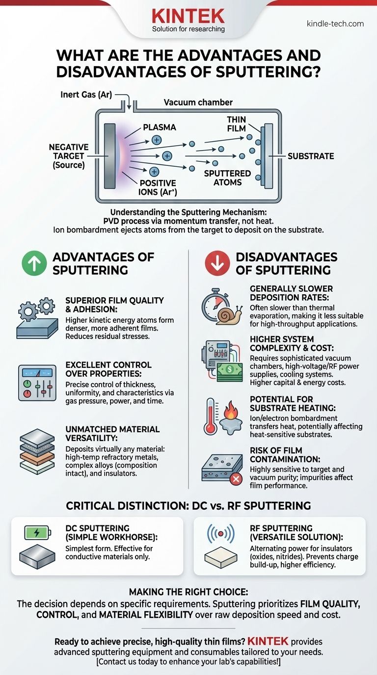
Understanding the Sputtering Mechanism
To grasp its pros and cons, you must first understand how sputtering works. It is a Physical Vapor Deposition (PVD) process that relies on momentum transfer, not heat.
The Core Principle: Ion Bombardment
A substrate and a source material (the "target") are placed in a vacuum chamber. The chamber is filled with a small amount of an inert gas, like argon.
A strong negative voltage is applied to the target, which ignites a plasma. The positively charged argon ions in the plasma are accelerated towards the negatively charged target.
These high-energy ions bombard the target with enough force to physically knock out, or "sputter," atoms from its surface. These sputtered atoms travel through the vacuum and deposit onto the substrate, building a thin film one atom at a time.
Key Advantages of Sputtering
Sputtering is often the go-to method when the quality and properties of the deposited film are more critical than the speed of production.
Superior Film Quality and Adhesion
Because sputtered atoms arrive at the substrate with higher kinetic energy than in thermal evaporation, they form denser, more adherent films. This process can also reduce residual stresses on the substrate, which is crucial for sensitive applications.
Excellent Control Over Film Properties
Sputtering allows for precise and repeatable control over film thickness and uniformity. By adjusting parameters like gas pressure, power, and deposition time, you can fine-tune the final film characteristics. Substrates can also be cleaned via ion bombardment within the chamber just before deposition, ensuring a pristine interface for better adhesion.
Unmatched Material Versatility
This is arguably sputtering's greatest strength. Unlike thermal evaporation, which is limited by a material's melting point, sputtering can deposit virtually any material. This includes high-temperature refractory metals, complex alloys (which deposit with their composition intact), and even insulating compounds.
Understanding the Trade-offs and Disadvantages
The control and versatility of sputtering come with clear operational costs and limitations that must be considered.
Generally Slower Deposition Rates
While modern techniques have improved speeds, basic sputtering is often slower than other methods like thermal evaporation. This can make it less suitable for high-throughput, low-cost applications where speed is the primary driver.
Higher System Complexity and Cost
Sputtering systems require sophisticated vacuum chambers, high-voltage power supplies, and often, cooling systems to manage heat. RF power supplies, necessary for sputtering insulating materials, are particularly expensive compared to the DC sources used for conductive materials. This leads to higher capital investment and energy costs.
Potential for Substrate Heating
The constant bombardment of energetic particles (ions, electrons, and sputtered atoms) can transfer a significant amount of heat to the substrate. While often less severe than in other processes, this can be a problem for heat-sensitive substrates like plastics or certain biological samples.
Risk of Film Contamination
The process is highly sensitive to the purity of both the target material and the vacuum environment. Any impurities in the target or residual gas in the chamber can be incorporated into the growing film, affecting its performance.
A Critical Distinction: DC vs. RF Sputtering
Not all sputtering is the same. The type of power source used fundamentally changes the process's capabilities.
DC Sputtering: The Simple Workhorse
Direct Current (DC) sputtering is the simplest form. It is highly effective and widely used but can only deposit electrically conductive materials. Attempting to sputter an insulator with DC power results in a build-up of positive charge on the target surface, which repels the incoming ions and stops the process.
RF Sputtering: The Versatile Solution
Radio Frequency (RF) sputtering uses an alternating power source. This alternating field prevents charge build-up on the target surface, making it possible to sputter insulating materials like oxides and nitrides. RF sputtering also tends to create a more efficient plasma, which can lead to higher deposition rates at lower pressures compared to basic DC sputtering.
Making the Right Choice for Your Goal
The decision to use sputtering depends entirely on your specific requirements for film quality, material type, and production volume.
- If your primary focus is high-performance films: Sputtering is the superior choice for depositing dense, adherent films from complex alloys, refractory metals, or compounds where stoichiometry is critical.
- If your primary focus is depositing insulators: RF sputtering is one of the most reliable and controllable methods for creating high-quality optical or dielectric films.
- If your primary focus is high-throughput and low cost: For simple metal coatings, thermal evaporation is often faster and more economical than sputtering.
Ultimately, choosing sputtering means prioritizing film quality, control, and material flexibility over raw deposition speed and cost.
Summary Table:
| Advantages | Disadvantages |
|---|---|
| Superior film adhesion & density | Lower deposition rates |
| Excellent control over film properties | Higher equipment cost & complexity |
| Deposits alloys, metals & insulators | Potential for substrate heating |
| High-quality, uniform films | Risk of film contamination |
Ready to achieve precise, high-quality thin films for your laboratory?
At KINTEK, we specialize in providing advanced sputtering equipment and consumables tailored to your specific research and production needs. Whether you're depositing complex alloys, refractory metals, or insulating compounds, our solutions deliver the superior control and material versatility your work demands.
Let our experts help you optimize your thin film processes. Contact us today to discuss how KINTEK can enhance your lab's capabilities!
Visual Guide
Related Products
- Spark Plasma Sintering Furnace SPS Furnace
- Vacuum Induction Melting Spinning System Arc Melting Furnace
- Chemical Vapor Deposition CVD Equipment System Chamber Slide PECVD Tube Furnace with Liquid Gasifier PECVD Machine
- Customer Made Versatile CVD Tube Furnace Chemical Vapor Deposition Chamber System Equipment
People Also Ask
- What are the advantages of CAMI/SPS for W-Cu composite preparation? Reduce cycles from hours to seconds.
- What is the mechanism of SPS process? A Deep Dive into Rapid, Low-Temperature Sintering
- What is the difference between spark plasma sintering and flash sintering? A Guide to Advanced Sintering Methods
- What is SPS sintering method? A Guide to High-Speed, High-Performance Material Fabrication
- What is the theory of spark plasma sintering? A Guide to Rapid, Low-Temperature Densification


