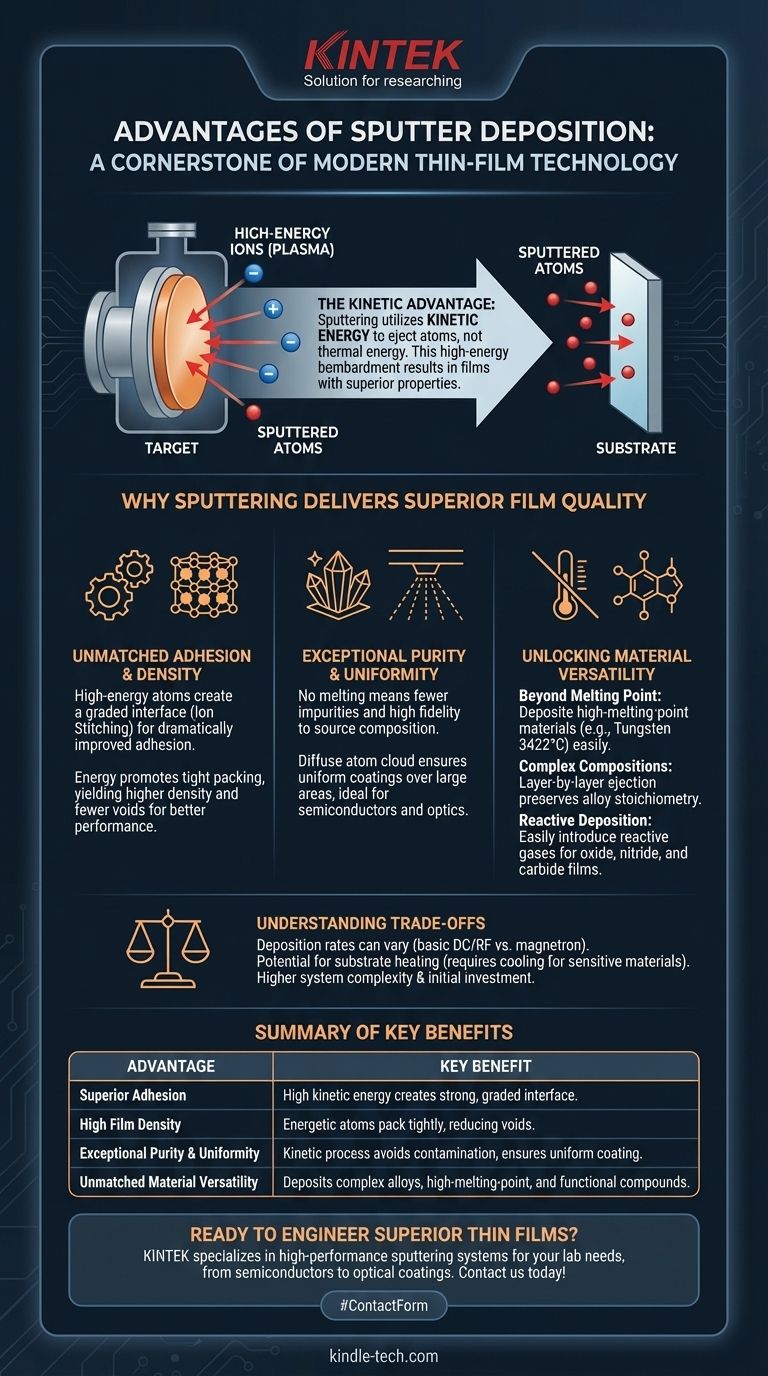
Sputter deposition is a cornerstone of modern thin-film technology because it offers exceptional control over a film’s physical properties. Unlike thermal methods that rely on melting, sputtering uses kinetic energy to eject atoms from a source material, resulting in superior adhesion, higher film density, and the ability to deposit a virtually unlimited range of materials, including complex alloys and high-melting-point compounds.
The core advantage of sputtering stems from a single principle: it is a physical, kinetic process, not a thermal one. This use of ion bombardment to eject atoms gives sputtered films higher energy, which translates directly into better adhesion, density, and purity compared to methods that rely on simple evaporation.
Why Sputtering Delivers Superior Film Quality
The quality of a thin film is defined by its adhesion to the substrate, its density, and its uniformity. Sputtering provides fundamental advantages in all three areas.
The Role of High Kinetic Energy
Sputtering works by bombarding a source material (the "target") with high-energy ions in a plasma. This collision physically ejects, or "sputters," atoms from the target.
These ejected atoms travel with significantly higher kinetic energy (typically 1-10 eV) than atoms from a thermal evaporation source (<1 eV). This energy is the key to sputtering's performance.
Unmatched Adhesion and Density
When high-energy sputtered atoms arrive at the substrate, they can physically implant themselves into the top atomic layers. This process, known as ion stitching, creates a graded interface and dramatically improves film adhesion.
This energy also promotes surface mobility, allowing atoms to settle into more tightly packed, ordered structures. The result is a film with higher density and fewer voids, leading to better barrier properties and electrical performance.
Exceptional Purity and Uniformity
Because sputtering does not require melting the source material, it introduces far fewer impurities. The process maintains the composition of the source material with high fidelity, making it ideal for depositing complex alloys and compounds.
The diffuse nature of the sputtered atom cloud and the ability to rotate the substrate ensures a highly uniform coating over large areas, which is critical for applications like semiconductor manufacturing and optical coatings.
Unlocking Material Versatility
While film quality is paramount, a deposition technique is only useful if it can handle the required materials. This is another area where sputtering's physical mechanism provides a decisive edge.
Beyond the Melting Point
Thermal evaporation is limited by a material's melting and boiling points. Materials with extremely high melting points, such as tungsten (3422°C) or tantalum (3017°C), are nearly impossible to evaporate effectively.
Sputtering bypasses this limitation entirely. Since it is a momentum-transfer process, any material that can be formed into a target can be sputtered, regardless of its melting point.
Preserving Complex Compositions
When a complex alloy is heated for thermal evaporation, the constituent elements will evaporate at different rates based on their individual vapor pressures. This leads to a film composition that does not match the source.
Sputtering, however, ejects atoms from the target surface layer by layer. This ensures the composition of the deposited film remains very close to the stoichiometry of the source target.
Reactive Deposition Made Simple
Sputtering allows for the easy introduction of reactive gases (like oxygen or nitrogen) into the vacuum chamber.
By sputtering a pure metal target in a reactive atmosphere, you can precisely form compound films like oxides, nitrides, and carbides on the substrate. This is a highly controllable method for creating functional ceramic coatings.
Understanding the Trade-offs
No technique is perfect for every scenario. Understanding the limitations of sputtering is crucial for making an informed decision.
Deposition Rates Can Vary
While modern magnetron sputtering offers very high deposition rates suitable for industrial production, basic DC or RF sputtering can be slower than thermal evaporation for some materials. The choice of sputtering configuration is critical for balancing speed and cost.
Potential for Substrate Heating
Although sputtering is considered a "low-temperature" process compared to methods like Chemical Vapor Deposition (CVD), the constant bombardment of the substrate by high-energy particles can induce heating. For extremely temperature-sensitive substrates, this must be managed with active cooling.
System Complexity
A sputtering system is inherently more complex than a simple thermal evaporator. It requires a robust vacuum system, high-voltage power supplies, and precise gas flow control, which can translate to a higher initial capital investment.
Making the Right Choice for Your Goal
Selecting sputter deposition depends entirely on the required properties of your final film.
- If your primary focus is maximum film adhesion and density: Sputtering is the superior choice for creating durable, high-performance coatings for demanding mechanical or electronic applications.
- If your primary focus is depositing a complex alloy or high-melting-point material: Sputtering is often the only viable PVD method, as it cleanly bypasses the challenges of thermal evaporation.
- If your primary focus is creating highly pure and uniform functional films: Sputtering provides unmatched control over stoichiometry and thickness, making it ideal for optics, semiconductors, and sensors.
Ultimately, understanding that sputtering leverages kinetic energy empowers you to choose the right tool for creating films with precisely engineered properties.
Summary Table:
| Advantage | Key Benefit |
|---|---|
| Superior Adhesion | High kinetic energy creates a strong, graded interface with the substrate. |
| High Film Density | Energetic atoms pack tightly, resulting in fewer voids and better performance. |
| Exceptional Purity & Uniformity | Kinetic process avoids contamination; provides uniform coating over large areas. |
| Unmatched Material Versatility | Deposits complex alloys, high-melting-point materials, and functional compounds. |
Ready to Engineer Superior Thin Films with Sputter Deposition?
At KINTEK, we specialize in providing high-performance lab equipment, including advanced sputtering systems, to meet the precise needs of your laboratory. Whether you are developing semiconductors, optical coatings, or durable functional films, our solutions deliver the critical advantages of superior adhesion, density, and material versatility.
Contact us today using the form below to discuss how our sputter deposition technology can enhance your research and production capabilities. Let KINTEK be your partner in achieving precisely engineered thin-film properties.
Visual Guide