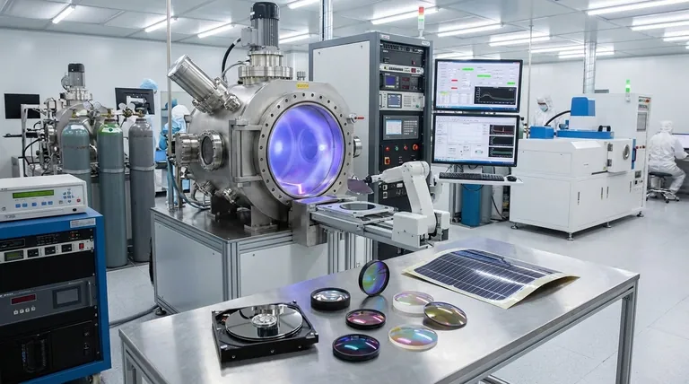
In short, sputter deposition is a foundational technology used to create the high-performance thin films essential for modern electronics and optics. Its primary applications are in the semiconductor industry for integrated circuits, in data storage for manufacturing hard disk drives, and in optics for creating specialized coatings on lenses and mirrors.
Sputter deposition is not just a coating method; it is a precision engineering tool. Its true value lies in its ability to deposit a vast range of materials—including complex alloys and high-melting-point compounds—with exceptional control, uniformity, and adhesion.
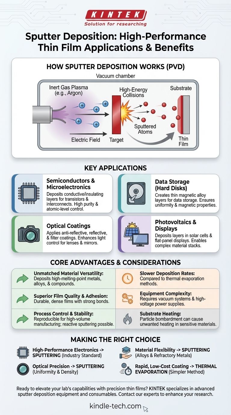
How Sputter Deposition Works
The Core Mechanism
Sputter deposition is a type of Physical Vapor Deposition (PVD). It works by creating a plasma, typically from an inert gas like argon, inside a vacuum chamber.
Positively charged argon ions from this plasma are accelerated by an electric field, causing them to collide with a target made of the desired coating material.
From Target to Substrate
These high-energy collisions physically knock off, or "sputter," individual atoms from the target material. These sputtered atoms then travel through the vacuum and condense onto the surface of a component (the substrate), forming a thin, uniform film.
Key Applications in Detail
Semiconductors and Microelectronics
Sputter deposition is a cornerstone of the semiconductor industry. It is used to deposit the ultra-thin layers of conductive and insulating materials that form transistors and interconnects within an integrated circuit.
The process offers the high purity and atomic-level control necessary to build these complex, multi-layered devices reliably and at scale.
Data Storage (Hard Disks)
One of the earliest and most critical applications of sputtering is in the production of computer hard disks. The magnetic layers that store data on a disk platter are just a few nanometers thick.
Sputtering is the only practical method to deposit these complex magnetic alloys with the required uniformity and magnetic properties.
Optical Coatings
The technology is essential for manufacturing high-performance optical components. It is used to apply anti-reflective coatings to lenses, create highly reflective mirrors, and produce specialized optical filters.
The dense, uniform films created by sputtering precisely control how light is reflected or transmitted, enhancing the performance of everything from eyeglasses to advanced scientific instruments.
Photovoltaics and Displays
In the renewable energy sector, sputtering is used to deposit various layers within solar cells (photovoltaics). It is also used in the manufacturing of flat-panel displays, contributing to the conductive and emissive layers.
Understanding the Core Advantages
Unmatched Material Versatility
A key advantage is the ability to deposit materials with very high melting points, such as tungsten or tantalum, which are difficult or impossible to deposit using thermal evaporation methods.
Furthermore, sputtering can deposit alloys and compounds while preserving the original composition of the target material, ensuring the final film has the desired chemical properties.
Superior Film Quality and Adhesion
Sputtered films are known for their excellent adhesion to the substrate. The high kinetic energy of the arriving atoms helps them form a strong, dense bond with the surface.
This results in durable, high-quality films that are less prone to peeling or defects compared to other methods.
Process Control and Stability
The sputtering target acts as a stable, long-lived source of material, leading to a highly reproducible and controllable process.
This stability is critical for high-volume manufacturing where consistency from one component to the next is paramount. It also allows for reactive sputtering, where a reactive gas like oxygen or nitrogen is introduced to form oxide or nitride compounds on the substrate.
Common Pitfalls and Considerations
Deposition Rates
Sputter deposition rates are often slower than those achieved with thermal evaporation. This can make it less suitable for applications where very thick films are needed quickly or where high throughput is the absolute primary concern.
Process Complexity
While highly controllable, the equipment required for sputtering can be more complex and expensive than simpler deposition techniques. It requires a vacuum system, high-voltage power supplies, and gas flow control, which demands a higher level of process expertise.
Substrate Heating
Although there is very little radiant heat from the source itself, the bombardment of the substrate by high-energy particles can cause some unwanted heating. This can be a concern when coating temperature-sensitive materials, such as plastics or biological samples.
Making the Right Choice for Your Goal
Sputter deposition is a powerful tool, but its suitability depends entirely on your project's technical requirements.
- If your primary focus is high-performance electronics: Sputtering is the industry standard for its ability to create the pure, dense, and complex material stacks needed for modern microchips.
- If your primary focus is optical precision: The uniformity and density of sputtered films are ideal for creating high-quality anti-reflective coatings, mirrors, and filters.
- If your primary focus is material flexibility: Sputtering is your best choice for depositing alloys, compounds, or refractory metals that cannot be handled by thermal methods.
- If your primary focus is rapid, low-cost coating: A simpler method like thermal evaporation may be a more appropriate choice, provided you do not need the superior film quality of sputtering.
Ultimately, choosing sputter deposition is a decision to prioritize film quality, material versatility, and process control above all else.
Summary Table:
| Application Area | Key Use | Key Material Benefit |
|---|---|---|
| Semiconductors | Depositing conductive & insulating layers for ICs | High purity, atomic-level control |
| Data Storage | Manufacturing magnetic layers for hard disk drives | Uniformity, precise magnetic properties |
| Optical Coatings | Creating anti-reflective, reflective layers on lenses/mirrors | Dense, uniform films for light control |
| Photovoltaics/Displays | Depositing layers in solar cells and flat-panel displays | Versatility for complex material stacks |
Ready to elevate your lab's capabilities with precision thin films? KINTEK specializes in advanced sputter deposition equipment and consumables, delivering the material versatility, superior adhesion, and process control your laboratory needs for semiconductors, optics, and beyond. Contact our experts today to discuss how our solutions can enhance your research and manufacturing outcomes.
Visual Guide
Related Products
- Chemical Vapor Deposition CVD Equipment System Chamber Slide PECVD Tube Furnace with Liquid Gasifier PECVD Machine
- HFCVD Machine System Equipment for Drawing Die Nano-Diamond Coating
- RF PECVD System Radio Frequency Plasma-Enhanced Chemical Vapor Deposition RF PECVD
- 915MHz MPCVD Diamond Machine Microwave Plasma Chemical Vapor Deposition System Reactor
- Customer Made Versatile CVD Tube Furnace Chemical Vapor Deposition Chamber System Equipment
People Also Ask
- What types of substrates are used in CVD to facilitate graphene films? Optimize Graphene Growth with the Right Catalyst
- How are carbon nanotubes grown? Master Scalable Production with Chemical Vapor Deposition
- Why is Chemical Vapor Deposition (CVD) equipment uniquely suited for constructing hierarchical superhydrophobic structures?
- How expensive is chemical vapor deposition? Understanding the True Cost of High-Performance Coating
- What are the core advantages of PE-CVD in OLED encapsulation? Protect Sensitive Layers with Low-Temp Film Deposition


