Sputtering deposition is a cornerstone technology used to create high-performance thin films across numerous industries. Its primary applications include the manufacturing of integrated circuits, the creation of anti-reflective coatings on glass, the application of hard, protective layers on cutting tools, and the production of reflective surfaces for media like CDs and DVDs.
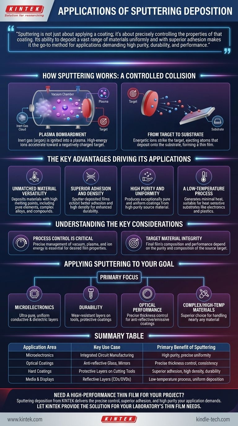
Sputtering is not just about applying a coating; it's about precisely controlling the properties of that coating. Its ability to deposit a vast range of materials uniformly and with superior adhesion makes it the go-to method for applications demanding high purity, durability, and performance.
How Sputtering Works: A Controlled Collision
The Core Mechanism: Plasma Bombardment
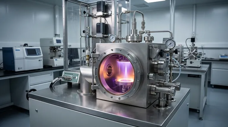
Sputtering is a type of Physical Vapor Deposition (PVD) that takes place inside a vacuum chamber. The process begins by introducing an inert gas, typically argon.
A high voltage is applied, igniting the gas into a plasma, which is a cloud of positively charged ions and free electrons.
These high-energy positive ions are accelerated toward a source material, known as the target, which is held at a negative charge.
From Target to Substrate
When the energetic ions strike the target, they physically knock off or "sputter" individual atoms from its surface.
These ejected atoms then travel through the vacuum chamber and deposit onto the component being coated, called the substrate, forming a thin, highly controlled film.
The Key Advantages Driving Its Applications
Unmatched Material Versatility
Sputtering can deposit materials with extremely high melting points, which are impossible to work with using traditional thermal evaporation methods.
This allows for the deposition of a wide range of materials, including pure elements, complex alloys, and compounds, making it essential for advanced manufacturing.
Superior Adhesion and Density
Sputter-deposited films typically exhibit better adhesion to the substrate compared to evaporated films.
The resulting coatings are also high-density, which translates directly to enhanced durability and longevity, critical for applications like protective layers on cutting tools.
High Purity and Uniformity
Because the film's composition is nearly identical to the high-purity source material, sputtering produces exceptionally pure and uniform coatings.
This capability is vital for the semiconductor industry, where even minute impurities can ruin an integrated circuit, and for optical coatings that require perfect consistency.
A Low-Temperature Process
The sputtering process generates very little radiant heat. This is a significant advantage as it prevents thermal damage to sensitive substrates.
This low-temperature nature makes it suitable for coating heat-sensitive electronics or plastics, such as those used in CDs and DVDs.
Understanding the Key Considerations
Process Control is Critical
The success of sputtering relies on precise control over the vacuum environment, plasma density, and ion energy. It is not a simple coating method.
Achieving the desired film properties, such as adhesion and density, requires careful management of these complex process parameters.
Target Material Integrity
The final film's composition is a direct reflection of the source target.
This means that the target material must be of exceptionally high purity and the correct chemical composition to ensure the performance of the final product. The process faithfully reproduces the source, for better or worse.
Applying Sputtering to Your Goal
To determine if sputtering is the right choice, consider the primary requirement of your component.
- If your primary focus is microelectronics: Sputtering is essential for depositing the ultra-pure, uniform conductive and dielectric layers required for integrated circuits.
- If your primary focus is durability: The superior adhesion and high density of sputtered films make it ideal for creating wear-resistant layers on tools or protective coatings on glass.
- If your primary focus is optical performance: Sputtering provides the precise thickness control and uniformity needed for high-performance anti-reflective or emissive coatings.
- If your primary focus is depositing complex or high-temperature materials: Sputtering is the superior choice over thermal methods for its ability to handle nearly any material regardless of its melting point.
Ultimately, sputtering excels wherever precise control over a film's composition, adhesion, and uniformity is paramount to the final product's performance.
Summary Table:
| Application Area | Key Use Case | Primary Benefit of Sputtering |
|---|---|---|
| Microelectronics | Integrated Circuit Manufacturing | High purity, precise uniformity |
| Optical Coatings | Anti-reflective Glass, Mirrors | Precise thickness control, consistency |
| Hard Coatings | Protective Layers on Cutting Tools | Superior adhesion, high density, durability |
| Media & Displays | Reflective Layers (CDs/DVDs) | Low-temperature process, uniform deposition |
Need a high-performance thin film for your project?
Sputtering deposition from KINTEK delivers the precise control, superior adhesion, and high purity your application demands. Whether you're developing advanced microelectronics, durable protective coatings, or high-quality optical layers, our expertise in lab equipment and consumables ensures your success.
Let KINTEK provide the solution for your laboratory's thin film needs.
Contact our experts today to discuss how we can support your specific application!
Visual Guide
Related Products
- Chemical Vapor Deposition CVD Equipment System Chamber Slide PECVD Tube Furnace with Liquid Gasifier PECVD Machine
- Customer Made Versatile CVD Tube Furnace Chemical Vapor Deposition Chamber System Equipment
- HFCVD Machine System Equipment for Drawing Die Nano-Diamond Coating
- RF PECVD System Radio Frequency Plasma-Enhanced Chemical Vapor Deposition RF PECVD
- 915MHz MPCVD Diamond Machine Microwave Plasma Chemical Vapor Deposition System Reactor
People Also Ask
- What are the processes of vapor phase deposition? Understand CVD vs. PVD for Superior Thin Films
- What are the advantages of chemical vapor deposition? Achieve Superior Thin Films for Your Lab
- How expensive is chemical vapor deposition? Understanding the True Cost of High-Performance Coating
- How are carbon nanotubes grown? Master Scalable Production with Chemical Vapor Deposition
- What happens during deposition chemistry? Building Thin Films from Gaseous Precursors


