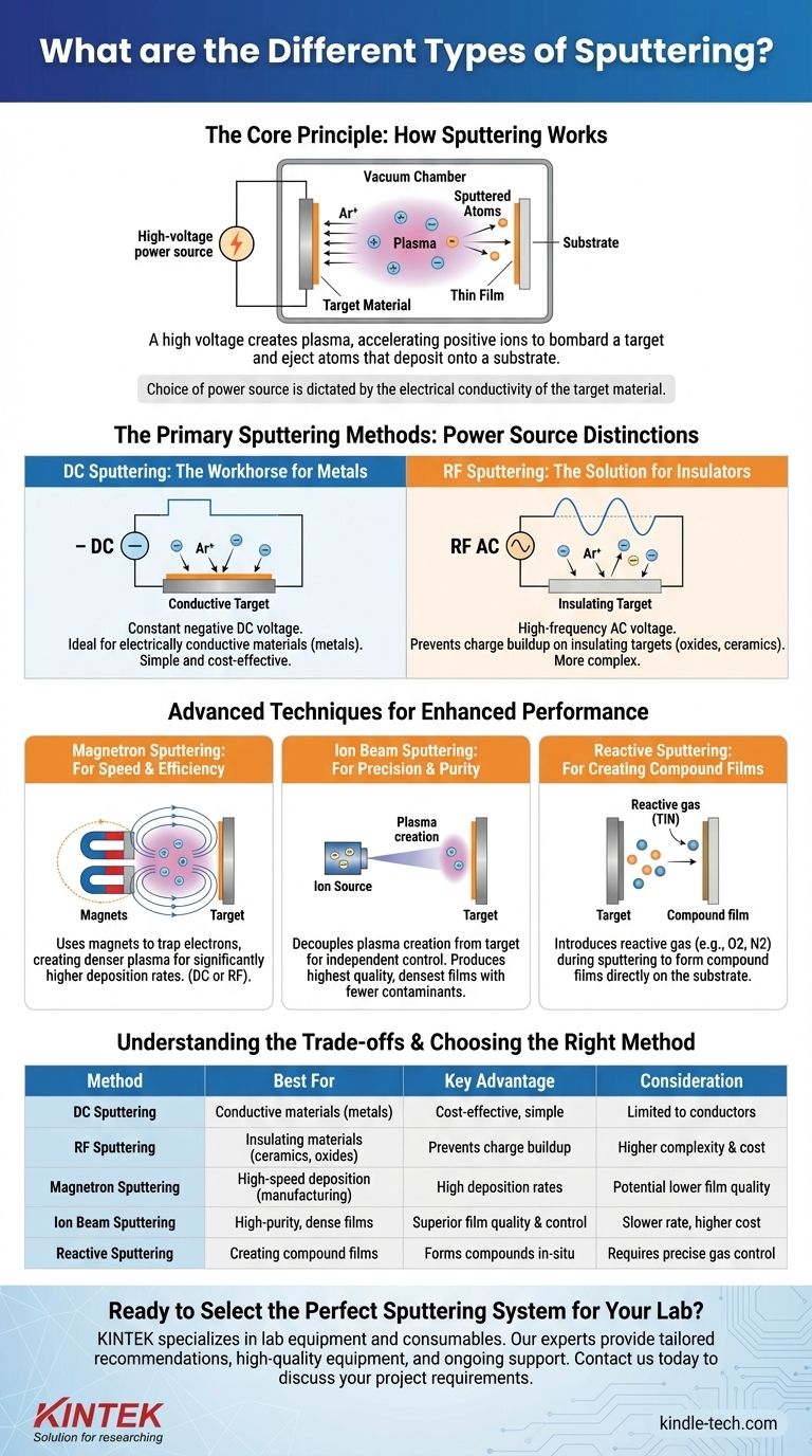
At its core, the different types of sputtering are distinguished by the power source used to create the plasma and the specific configuration of the system. The two primary methods are DC (Direct Current) Sputtering, which is ideal for electrically conductive materials like metals, and RF (Radio Frequency) Sputtering, which is necessary for depositing non-conductive, insulating materials.
The choice between sputtering techniques is not arbitrary; it is fundamentally dictated by the electrical conductivity of the target material you intend to deposit. Advanced methods like magnetron or ion beam sputtering are then layered on top to enhance speed, control, and film quality.
The Core Principle: How Sputtering Works
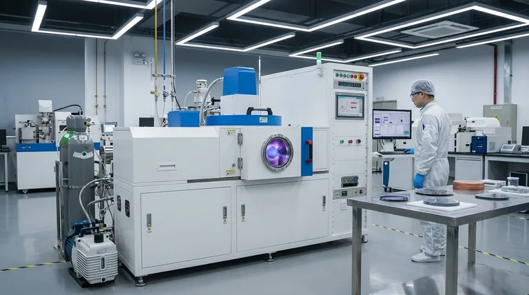
Sputtering is a physical vapor deposition (PVD) process used to deposit extremely thin films of material onto a surface, or substrate. It offers exceptional film adhesion and thickness control.
The Basic Mechanism
A high voltage is applied within a vacuum chamber filled with an inert gas, typically Argon. This voltage ignites the gas into a plasma, a state of matter containing positive ions and free electrons.
These positively charged gas ions are accelerated towards a source material, known as the target. The energetic ions bombard the target with enough force to knock off, or "sputter," individual atoms.
These sputtered atoms then travel through the chamber and deposit onto the substrate, building a thin, uniform film layer by layer.
The Primary Sputtering Methods
The fundamental difference between sputtering types comes from the power supply used to generate and sustain the plasma. This choice directly impacts which materials can be deposited.
DC Sputtering: The Workhorse for Metals
In DC sputtering, a constant negative DC voltage is applied to the target. This continuously attracts the positive Argon ions, leading to a steady sputtering process.
Because it relies on a constant flow of charge, DC sputtering is only effective for electrically conductive targets, primarily metals. A charge buildup on an insulating target would quickly halt the process.
RF Sputtering: The Solution for Insulators
RF sputtering uses a high-frequency AC voltage instead of a DC source. This alternating field rapidly switches the target's polarity from negative to positive.
During the negative cycle, ion bombardment and sputtering occur as normal. During the brief positive cycle, the target attracts electrons from the plasma, which neutralize the positive charge that would otherwise accumulate on an insulating surface.
This key difference makes RF sputtering the necessary choice for depositing insulating (dielectric) materials like oxides and ceramics.
Advanced Techniques for Enhanced Performance
Beyond the choice of power supply, specialized system configurations are used to improve the sputtering process for specific goals like speed, film quality, or material composition.
Magnetron Sputtering: For Speed and Efficiency
This is the most common technique in modern industry. Magnetron sputtering adds powerful magnets behind the target.
These magnets trap free electrons in a magnetic field directly in front of the target. This dramatically increases the probability of electrons colliding with Argon gas atoms, creating a much denser, more intense plasma.
The result is a significantly higher sputtering rate and faster film deposition, making it ideal for manufacturing. Magnetron systems can be powered by either DC or RF sources.
Ion Beam Sputtering: For Precision and Purity
In an ion beam system, the plasma creation is separated from the target. A dedicated ion source generates a focused, controllable beam of ions that is then aimed at the target.
This decoupling allows for independent control over ion energy and current. It results in fewer contaminants and a more ordered film structure, producing the highest quality, densest films with minimal defects.
Reactive Sputtering: For Creating Compound Films
Reactive sputtering is a method for creating compound materials. It involves introducing a reactive gas, like oxygen or nitrogen, into the vacuum chamber along with the inert Argon.
As a metal target (e.g., titanium) is sputtered, its atoms react with the gas (e.g., nitrogen) on their way to the substrate. This process forms a compound film directly on the substrate, such as titanium nitride (TiN).
Understanding the Trade-offs
Each sputtering method comes with its own set of advantages and limitations, making the choice dependent on your specific application and desired outcome.
The Material Constraint
The single biggest factor is the material. If your target is conductive, you can use the simpler, less expensive DC sputtering setup. If your target is an insulator, you have no choice but to use RF sputtering.
Complexity and Cost
DC systems are relatively simple and cost-effective. RF systems are more complex, requiring an impedance-matching network to efficiently transfer power to the plasma, which increases cost and operational difficulty.
Rate vs. Quality
Magnetron sputtering offers the highest deposition rates, but the film quality may be lower than that achieved with other methods. Ion beam sputtering provides a lower deposition rate but offers unparalleled control over film properties, density, and purity.
Choosing the Right Sputtering Method
Your choice of technique should be a direct reflection of your material, budget, and the desired properties of your final thin film.
- If your primary focus is depositing a simple metal film cost-effectively: A standard DC sputtering system is the most direct and efficient choice.
- If your primary focus is depositing an insulator, ceramic, or polymer: An RF sputtering system is required to prevent charge accumulation on the target.
- If your primary focus is high-speed deposition for manufacturing: DC or RF Magnetron sputtering is the industry standard for its high throughput.
- If your primary focus is achieving the highest possible film purity and density: Ion beam sputtering offers the ultimate level of control, albeit at a slower rate.
- If your primary focus is creating a specific compound like an oxide or nitride: Reactive sputtering is the designated technique for forming compound films in-situ.
Ultimately, understanding these methods empowers you to select the right tool to precisely control the growth and properties of your thin film.
Summary Table:
| Method | Best For | Key Advantage |
|---|---|---|
| DC Sputtering | Conductive materials (metals) | Cost-effective, simple operation |
| RF Sputtering | Insulating materials (ceramics, oxides) | Prevents charge buildup on target |
| Magnetron Sputtering | High-speed deposition (manufacturing) | High deposition rates with dense plasma |
| Ion Beam Sputtering | High-purity, dense films (optics, semiconductors) | Superior film quality and control |
| Reactive Sputtering | Creating compound films (nitrides, oxides) | Forms compounds directly during deposition |
Ready to Select the Perfect Sputtering System for Your Lab?
Choosing the right sputtering technique is critical for achieving your desired thin film properties, whether you're working with conductive metals, insulating ceramics, or need high-purity deposition.
KINTEK specializes in lab equipment and consumables, serving laboratory needs. Our experts can help you navigate the complexities of DC, RF, magnetron, and ion beam sputtering to find the ideal solution for your specific application and budget.
We provide:
- Tailored Recommendations: Get expert guidance on the best sputtering method for your materials and research goals.
- High-Quality Equipment: Access reliable sputtering systems designed for precision and performance.
- Ongoing Support: Ensure your lab operates at peak efficiency with our comprehensive service and consumables.
Don't leave your thin film results to chance. Contact us today to discuss your project requirements and discover how KINTEK's sputtering solutions can advance your research or production.
Visual Guide
Related Products
- Spark Plasma Sintering Furnace SPS Furnace
- Vacuum Induction Melting Spinning System Arc Melting Furnace
- Chemical Vapor Deposition CVD Equipment System Chamber Slide PECVD Tube Furnace with Liquid Gasifier PECVD Machine
- Customer Made Versatile CVD Tube Furnace Chemical Vapor Deposition Chamber System Equipment
People Also Ask
- Why are Spark Plasma Sintering (SPS) furnaces or hot presses utilized in the preparation of Li3PS4 solid electrolytes?
- What is the pressure for spark plasma sintering? A Guide to Optimizing SPS Parameters
- What are the advantages of CAMI/SPS for W-Cu composite preparation? Reduce cycles from hours to seconds.
- What is the mechanism of SPS process? A Deep Dive into Rapid, Low-Temperature Sintering
- What is the process fundamentals of spark plasma sintering? Achieve Rapid, High-Density Material Consolidation


