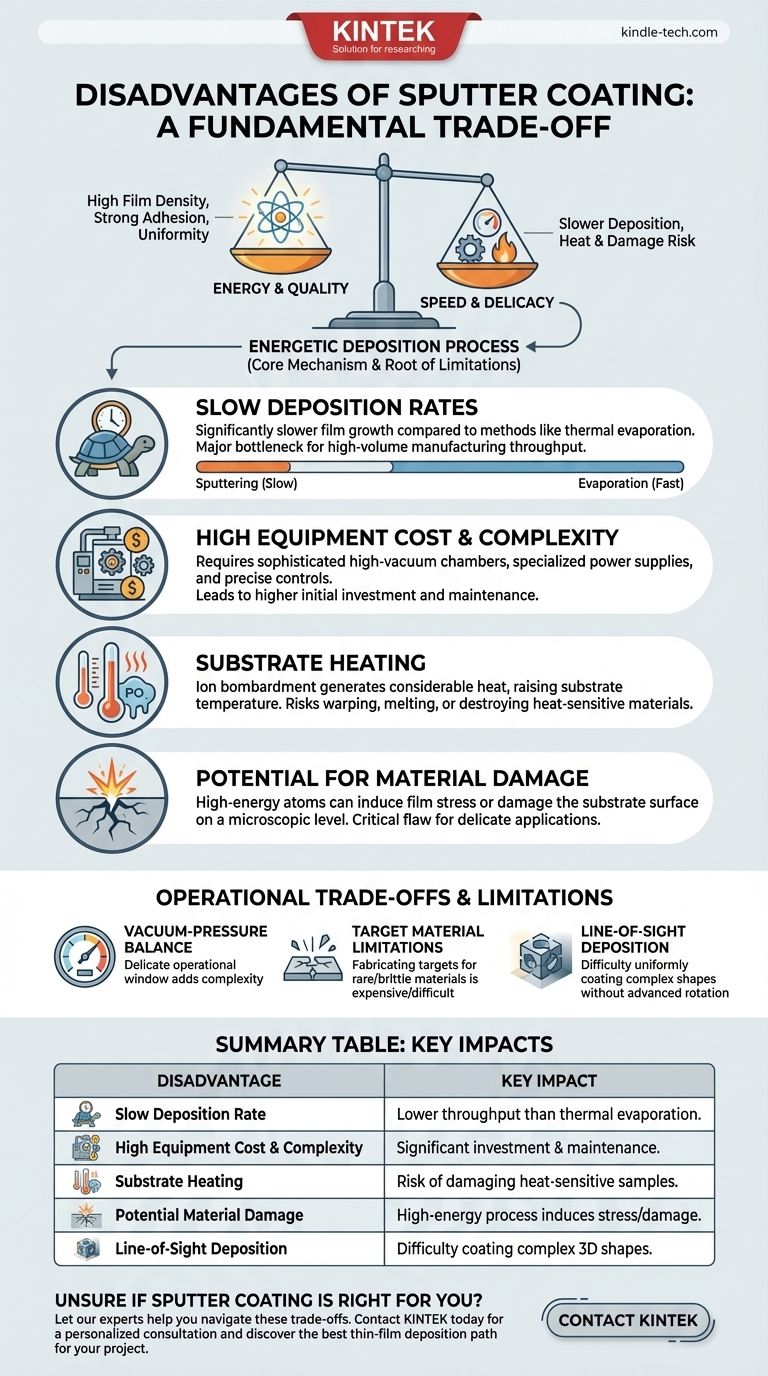
While remarkably effective for producing high-quality thin films, sputter coating is not without its drawbacks. Its primary disadvantages stem from slower deposition rates when compared to other methods, higher equipment complexity and cost, and the potential for unwanted substrate heating. The energetic nature of the process, which gives sputtered films their superior adhesion and density, can also introduce stress or damage to sensitive materials.
Sputter coating's greatest strengths—high film density, strong adhesion, and uniformity—are a direct result of its energetic, atom-by-atom deposition process. However, this same energetic nature is the source of its main drawbacks: slower speeds and potential heat damage to sensitive substrates.
A Fundamental Trade-off: Energy vs. Delicacy
To understand the disadvantages of sputter coating, we must first appreciate its core mechanism. The process is inherently energetic, which is both its biggest advantage and the root of its limitations.
The Principle of Energetic Deposition
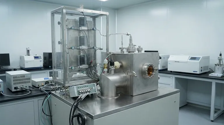
Sputtering uses energized ions (typically argon) in a vacuum to bombard a target material. This high-energy collision physically ejects atoms from the target, which then travel and deposit onto a substrate, forming a thin film.
The Source of Its Strengths
This energetic, atom-by-atom deposition is why sputtering produces films with superior adhesion, high density, and excellent uniformity. The atoms arrive at the substrate with significant kinetic energy, allowing them to form a tightly packed, durable layer that other methods struggle to achieve.
The Primary Disadvantages of Sputter Coating
The same characteristics that produce high-quality films also create practical and physical limitations that must be considered for any application.
Slow Deposition Rates
Because material is ejected on an atomic level, the overall rate of film growth is often significantly slower than other methods, like thermal evaporation. This can be a major bottleneck in high-volume manufacturing environments where throughput is a critical metric.
High Equipment Cost and Complexity
Sputtering systems are sophisticated machines. They require a high-vacuum chamber, specialized high-voltage DC or RF power supplies to generate the plasma, and precise gas flow controllers. This complexity leads to higher initial investment and ongoing maintenance costs compared to simpler coating techniques.
Substrate Heating
The constant bombardment of the target by ions and the plasma itself generate considerable heat. This energy is transferred to the substrate, which can raise its temperature significantly. This is a major disadvantage when working with heat-sensitive materials like polymers, plastics, or biological samples, which can warp, melt, or be destroyed.
Potential for Material Damage
The high energy of the depositing atoms can be a double-edged sword. While it promotes adhesion, it can also induce stress in the growing film or damage the substrate's surface on a microscopic level. For applications requiring a perfect, damage-free crystalline structure, such as in advanced semiconductors, this can be a critical flaw.
Understanding the Operational Trade-offs
Beyond the primary drawbacks, several operational factors introduce further trade-offs that require careful management.
The Vacuum-Pressure Balance
Sputtering requires a delicate balance. The chamber must be at a low enough pressure (a vacuum) for sputtered atoms to travel freely, but at a high enough pressure to sustain the argon plasma. Maintaining this narrow operational window adds to the process's complexity.
Target Material Limitations
The process requires the coating material to be fabricated into a solid, high-purity target. For some brittle, rare, or difficult-to-machine materials, creating a suitable sputtering target can be prohibitively expensive or technically challenging.
Line-of-Sight Deposition
While sputtered particles are not influenced by gravity, the process is still fundamentally line-of-sight. Coating complex, three-dimensional shapes with undercuts or hidden surfaces uniformly is difficult without sophisticated, multi-axis substrate rotation, further adding to system complexity.
Making the Right Choice for Your Goal
Selecting a deposition method requires weighing the need for film quality against practical constraints like speed, cost, and substrate compatibility.
- If your primary focus is high film quality and adhesion: Sputtering is often the superior choice, provided you can manage the slower speed and potential for substrate heating.
- If your primary focus is high-throughput and lower cost: You should evaluate alternative methods like thermal evaporation or electroplating, which may offer better speed and economy for less demanding applications.
- If you are working with heat-sensitive or delicate substrates: Proceed with caution, as you may need specialized cooling systems or should strongly consider less energetic deposition techniques.
Ultimately, understanding these trade-offs is the key to leveraging sputter coating's power where it matters most.
Summary Table:
| Disadvantage | Key Impact |
|---|---|
| Slow Deposition Rate | Lower throughput compared to methods like thermal evaporation. |
| High Equipment Cost & Complexity | Significant initial investment and maintenance for vacuum systems and power supplies. |
| Substrate Heating | Risk of damaging heat-sensitive materials like polymers or biological samples. |
| Potential Material Damage | High-energy process can induce film stress or damage delicate substrates. |
| Line-of-Sight Deposition | Difficulty uniformly coating complex 3D shapes without advanced rotation systems. |
Unsure if sputter coating is right for your lab's specific materials and throughput needs?
The disadvantages of high cost, slow speed, and substrate heating are significant, but so are the advantages of superior film adhesion and density. The right choice depends on your precise application. KINTEK specializes in lab equipment and consumables, serving laboratory needs with expert advice and tailored solutions.
Let our experts help you navigate these trade-offs. We can help you determine the optimal thin-film deposition technique for your research or production goals, ensuring you get the quality you need without unnecessary cost or complexity.
Contact KINTEK today for a personalized consultation and discover the best path forward for your project.
Visual Guide
Related Products
- Custom CVD Diamond Coating for Lab Applications
- HFCVD Machine System Equipment for Drawing Die Nano-Diamond Coating
- Chemical Vapor Deposition CVD Equipment System Chamber Slide PECVD Tube Furnace with Liquid Gasifier PECVD Machine
- Multifunctional Electrolytic Electrochemical Cell Water Bath Single Layer Double Layer
- Professional Cutting Tools for Carbon Paper Cloth Diaphragm Copper Aluminum Foil and More
People Also Ask
- How thick is CVD diamond coating? Balancing Durability and Stress for Optimal Performance
- What is CVD coated? A Guide to Superior Wear Resistance for Complex Parts
- What is CVD coating? Transform Your Material's Surface for Maximum Performance
- What are the different CVD coating? A Guide to Thermal CVD, PECVD, and Specialized Methods
- What is CVD diamond coating? Grow a Super-Hard, High-Performance Diamond Layer


