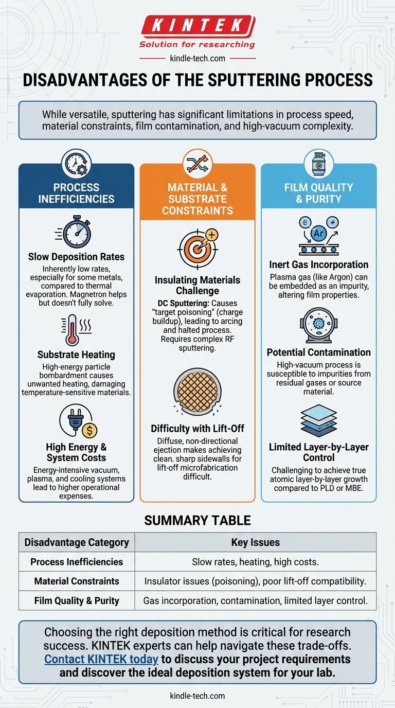
While sputtering is a highly versatile and widely used thin-film deposition technique, it is not without significant limitations. The primary disadvantages revolve around process speed, material constraints, potential for film contamination, and the inherent complexity and cost associated with a high-vacuum process.
Sputtering's core trade-off is its versatility versus its inherent physical limitations. The process is slower than simple evaporation, can introduce impurities into the film, and requires specific configurations (like RF sputtering) to handle insulating materials, making it a powerful but not universally perfect solution.
Process Inefficiencies and Rate Limitations
The physical nature of sputtering—ejecting atoms from a target with energetic ions—creates several practical inefficiencies that must be managed.
Slow Deposition Rates
While modern magnetron sputtering has significantly improved speeds, basic sputtering techniques have inherently low deposition rates. The process of ion bombardment and atom ejection is less efficient at transferring material than thermal evaporation for many common metals.
Substrate Heating
The substrate is bombarded by high-energy particles, including secondary electrons and sputtered atoms. This energy transfer can cause significant unwanted heating of the substrate, which can damage temperature-sensitive materials like polymers or delicate electronic devices.
High Energy and System Costs
Sputtering is an energy-intensive process. It requires power to maintain the vacuum, generate the plasma, and often run a cooling system to manage heat on both the target and substrate. This leads to higher operational costs compared to some non-vacuum or simpler thermal deposition methods.
Material and Substrate Constraints
Not all materials can be deposited easily or effectively with every type of sputtering, and the process itself can limit subsequent manufacturing steps.
The Challenge of Insulating Materials
This is the most significant limitation of the simplest sputtering method, DC Sputtering. When sputtering non-conductive (dielectric) materials, a positive charge builds up on the target surface, which eventually repels the positive ions from the plasma.
This phenomenon, known as target poisoning, can lead to arcing that damages the substrate or completely halts the deposition process. This requires the use of more complex and expensive techniques like RF (Radio Frequency) sputtering.
Difficulty with Lift-Off Processes
Sputtering ejects atoms from the target in a diffuse, non-directional manner. This makes it very difficult to achieve the clean, sharp sidewalls required for patterning films using a lift-off process, a common technique in microfabrication. Evaporation, which is a line-of-sight process, is far better suited for lift-off.
Understanding the Trade-offs: Film Quality and Purity
Achieving a pristine, high-quality film with sputtering requires careful control to mitigate sources of contamination and structural imperfections.
Inert Gas Incorporation
The inert gas used to create the plasma (typically Argon) can become embedded or incorporated into the growing thin film as an impurity. This contamination can alter the film's electrical, optical, and mechanical properties in undesirable ways.
Potential for System Contamination
Like any high-vacuum process, sputtering is susceptible to contamination. Impurities can arise from residual gases in the chamber or from the source material itself, impacting the purity of the final film.
Limited Layer-by-Layer Control
While sputtering provides excellent control over film thickness and uniformity, it is more challenging to achieve the true atomic layer-by-layer growth possible with techniques like Pulsed Laser Deposition (PLD) or Molecular Beam Epitaxy (MBE).
Making the Right Choice for Your Application
Understanding these disadvantages is key to selecting the right deposition method for your specific goal.
- If your primary focus is depositing simple conductive metals quickly and cheaply: Consider thermal evaporation, which is often faster and better suited for lift-off patterning.
- If your primary focus is depositing insulating materials like oxides or nitrides: You must use RF sputtering or a similar technique; basic DC sputtering is not a viable option due to target poisoning.
- If your primary focus is achieving the highest possible film purity and crystalline quality: Be aware of gas incorporation and consider alternatives like MBE for demanding epitaxial applications.
- If your primary focus is coating temperature-sensitive substrates: You must account for substrate heating and implement a robust cooling system or adjust deposition parameters to minimize thermal damage.
Ultimately, choosing the right deposition process requires a clear understanding of the trade-offs between speed, cost, material compatibility, and the final required quality of the film.
Summary Table:
| Disadvantage Category | Key Issues |
|---|---|
| Process Inefficiencies | Slow deposition rates, unwanted substrate heating, high energy and operational costs. |
| Material Constraints | Difficulty with insulating materials (target poisoning), poor compatibility with lift-off processes. |
| Film Quality & Purity | Inert gas incorporation, potential for system contamination, limited layer-by-layer control. |
Choosing the right deposition method is critical for your research success. The limitations of sputtering—such as speed, material compatibility, and cost—highlight the need for expert guidance to select the optimal equipment for your specific application, whether it's for metals, oxides, or temperature-sensitive substrates.
KINTEK specializes in lab equipment and consumables, serving laboratory needs. Our experts can help you navigate these trade-offs to find the most efficient and cost-effective thin-film solution for your work.
Contact KINTEK today to discuss your project requirements and discover the ideal deposition system for your lab.
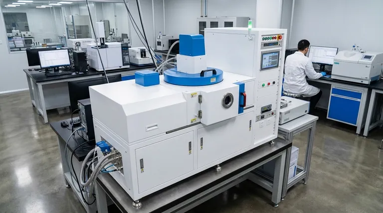
Visual Guide
Related Products
- Spark Plasma Sintering Furnace SPS Furnace
- Vacuum Induction Melting Spinning System Arc Melting Furnace
- Chemical Vapor Deposition CVD Equipment System Chamber Slide PECVD Tube Furnace with Liquid Gasifier PECVD Machine
- Customer Made Versatile CVD Tube Furnace Chemical Vapor Deposition Chamber System Equipment
People Also Ask
- What is the difference between spark plasma sintering and flash sintering? A Guide to Advanced Sintering Methods
- Why are Spark Plasma Sintering (SPS) furnaces or hot presses utilized in the preparation of Li3PS4 solid electrolytes?
- What is the process fundamentals of spark plasma sintering? Achieve Rapid, High-Density Material Consolidation
- What is the pressure for spark plasma sintering? A Guide to Optimizing SPS Parameters
- What is the mechanism of SPS process? A Deep Dive into Rapid, Low-Temperature Sintering


