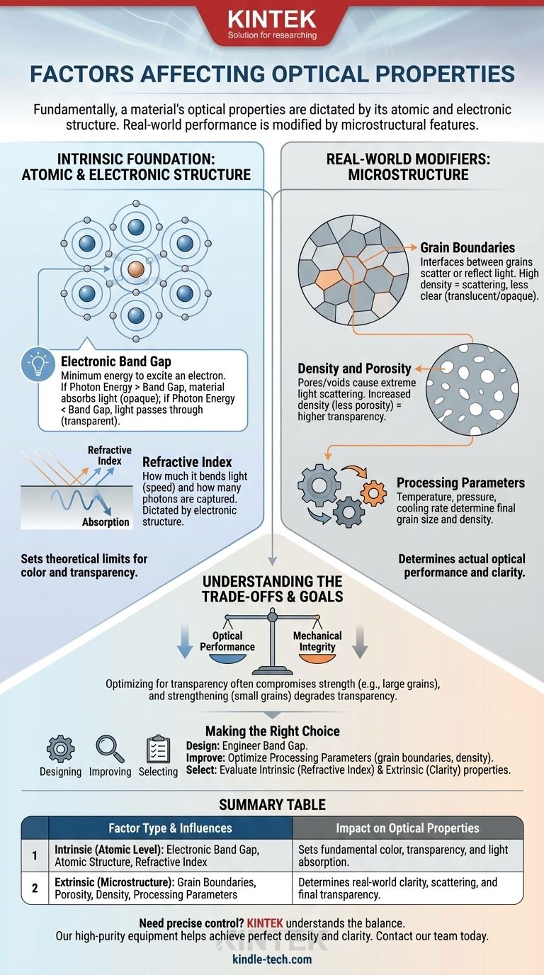
Fundamentally, a material's optical properties are dictated by its atomic and electronic structure. How a material responds to light is governed first by its inherent chemistry and the arrangement of its electrons. On a larger scale, its real-world performance—especially its transparency—is then modified by microstructural features like internal boundaries and overall density.
The way a material interacts with light is governed by two distinct levels. Intrinsic properties, like the material's fundamental band gap, set the theoretical limits for color and transparency, while extrinsic factors, such as grain boundaries from processing, determine the actual optical performance you observe.

The Intrinsic Foundation: Atomic and Electronic Structure
The baseline optical behavior of any material is set at the atomic level. These intrinsic properties are determined by the type of atoms present and how their electrons are organized.
The Critical Role of the Band Gap
The single most important factor is the electronic band gap. This is the minimum amount of energy required to excite an electron in the material to a higher energy state.
When light (a stream of photons) hits a material, if the photon's energy is less than the band gap energy, it cannot be absorbed and will pass through. This makes the material transparent.
If the photon's energy is greater than the band gap, it will be absorbed by an electron. This makes the material opaque. The specific colors absorbed determine the color we perceive.
Atomic Structure and Electron Interaction
The arrangement of atoms in a crystal lattice determines the shape and size of this band gap. Different crystal structures of the same element (allotropes) can have vastly different optical properties for this reason.
Refractive Index and Absorption
A material's refractive index—how much it bends light—is also a function of its electronic structure. It describes how the light wave's speed is slowed by its interaction with the material's electrons.
Absorption is a direct measure of how many photons are captured at a given energy or wavelength. Both refractive index and absorption are direct consequences of the material's band structure.
The Real-World Modifiers: Microstructure
Even if a material has an ideal band gap for transparency, its final form can make it opaque. This is where extrinsic, or microstructural, factors come into play.
Grain Boundaries and Light Scattering
Most real-world materials are polycrystalline, meaning they are composed of many small crystal grains. The interface between these grains is called a grain boundary.
Each grain boundary acts as a surface that can scatter or reflect light. A high density of grain boundaries will scatter light in all directions, preventing a clear image from passing through and making the material appear translucent or opaque, much like frosted glass.
The Influence of Density and Porosity
Pores or voids within a material are a major cause of opacity. Each pore is an interface between the material and air, which causes extreme light scattering.
Increasing a material's density to its theoretical maximum by eliminating porosity is critical for achieving high transparency in polycrystalline bodies.
How Processing Parameters Shape the Outcome
The way a material is manufactured directly controls its microstructure. Processing parameters like temperature, pressure, and cooling rate determine the final grain size and density.
For example, carefully selecting parameters for thin-film deposition can create a material with a low grain boundary density, resulting in desirable properties like a high refractive index and low absorption.
Understanding the Trade-offs
Optimizing for optical properties often involves balancing competing factors. It is crucial to recognize these limitations.
Intrinsic Limits vs. Practical Reality
A material can have a perfect band gap for transparency (an intrinsic property), but be rendered opaque if the manufacturing process creates a high density of grain boundaries or pores (extrinsic factors). You cannot overcome poor microstructure simply by having a good band gap.
Optical Performance vs. Mechanical Integrity
Often, the processes needed to create large, optically clear grains (like slow cooling) can result in a material that is more brittle or mechanically weaker. Conversely, strengthening a material by creating very small grains will almost always degrade its transparency due to increased light scattering at the numerous grain boundaries.
Making the Right Choice for Your Goal
Your approach should be dictated by your specific objective, whether you are designing, improving, or simply selecting a material.
- If your primary focus is designing a completely new transparent material: You must start by engineering the electronic band gap to be larger than the energy of visible light photons.
- If your primary focus is improving an existing material's transparency: Your effort should be on optimizing processing parameters to minimize grain boundaries and increase density.
- If your primary focus is selecting a material for an optical component: You must evaluate both its intrinsic properties (like refractive index from a datasheet) and its extrinsic quality (judged by its clarity and lack of scattering).
By understanding these factors from the atomic to the microstructural level, you gain direct control over how a material looks and performs.
Summary Table:
| Factor Type | Key Influences | Impact on Optical Properties |
|---|---|---|
| Intrinsic (Atomic Level) | Electronic Band Gap, Atomic Structure, Refractive Index | Sets fundamental color, transparency, and light absorption. |
| Extrinsic (Microstructure) | Grain Boundaries, Porosity, Density, Processing Parameters | Determines real-world clarity, scattering, and final transparency. |
Need precise control over your material's optical performance? The experts at KINTEK understand the intricate balance between atomic structure and manufacturing processes. Whether you're developing new transparent materials or optimizing existing ones, our high-purity lab equipment and consumables are designed to help you achieve the perfect density, grain size, and clarity.
Contact our team today to discuss how we can support your laboratory's specific optical material goals.
Visual Guide
