At its core, cathode sputtering is a highly controlled physical vapor deposition (PVD) process used to create ultra-thin films. In a vacuum, high-energy ions from a plasma bombard a source material—known as the target, which functions as the cathode (a negative electrode). This atomic-scale collision physically knocks atoms off the target, which then travel and deposit onto a substrate, forming a precise and uniform coating.
Sputtering is fundamentally a process of momentum transfer, not heat. It uses energetic ions as microscopic "billiard balls" to eject atoms from a solid target, allowing for the deposition of materials—especially those with very high melting points or complex compositions—that are difficult to coat using other methods.
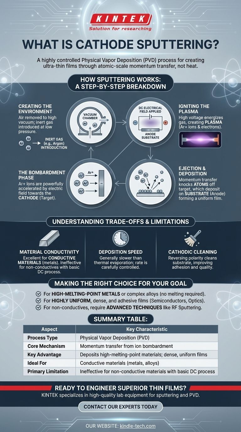
How Sputtering Works: A Step-by-Step Breakdown
To understand cathode sputtering, it's best to visualize it as a sequence of events occurring within a controlled environment. The entire process hinges on creating and directing a stream of energized particles.
Creating the Environment
The process begins in a vacuum chamber. All air and contaminants are pumped out to create a high-vacuum environment.
An inert gas, most commonly Argon (Ar), is then introduced into the chamber at a very low pressure.
Igniting the Plasma
A strong DC electrical field is applied, with the source material (the target) acting as the negative cathode and the object to be coated (the substrate) acting as the positive anode.
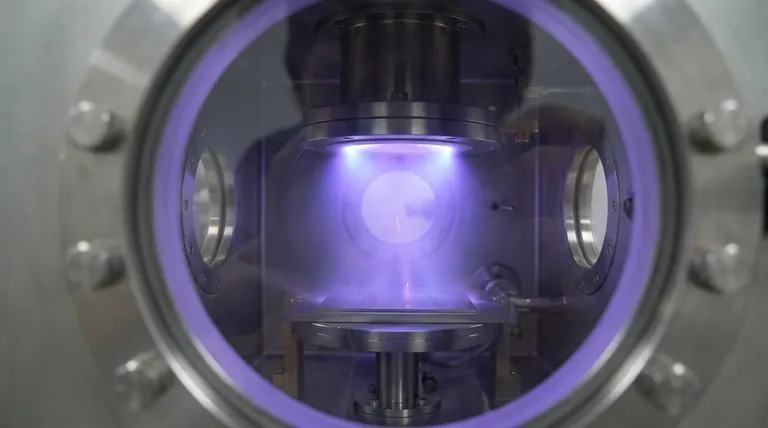
This high voltage energizes the argon gas, stripping electrons from the argon atoms and creating a plasma—an ionized gas containing positive argon ions (Ar+) and free electrons. This is often visible as a characteristic glow.
The Bombardment Phase
The positively charged argon ions (Ar+) are powerfully accelerated by the electric field and drawn toward the negatively charged target (cathode).
These high-energy ions collide with the surface of the target with significant force.
Ejection and Deposition
The impact's momentum is transferred to the atoms of the target material, causing them to be physically knocked out or "sputtered" from the surface.
These ejected target atoms travel through the vacuum chamber and condense on the surface of the substrate (anode), gradually building up a thin, uniform film.
Understanding the Trade-offs and Limitations
While powerful, the basic DC cathode sputtering process has specific constraints that are critical to understand when evaluating its suitability for an application.
Material Conductivity
The standard DC sputtering process works exceptionally well for conductive materials like metals.
However, it is ineffective for depositing non-conductive (dielectric or insulating) materials. Charge builds up on an insulating target surface, repelling the positive ions and eventually stopping the sputtering process. More advanced techniques, like RF sputtering, are required for these materials.
Deposition Speed
Sputtering can be a slower deposition method compared to other techniques like thermal evaporation. The rate of film growth is carefully controlled but often lower.
Cathodic Cleaning
A key advantage is the ability to reverse the polarity before deposition. This technique, known as cathodic cleaning or "sputter etching," uses the ions to clean contaminants from the substrate's surface, which dramatically improves the adhesion and quality of the final film.
Making the Right Choice for Your Goal
Deciding if sputtering is the correct deposition method depends entirely on your material, quality requirements, and application.
- If your primary focus is depositing high-melting-point metals or complex alloys: Sputtering is a superior choice because it does not rely on melting the source material.
- If your primary focus is creating highly uniform, dense, and adhesive films for semiconductors or optical devices: Sputtering offers exceptional control over film thickness and produces high-quality coatings.
- If your primary focus is coating a non-conductive material like a ceramic or polymer: You must look beyond basic DC sputtering to alternative methods or more advanced techniques like RF (Radio Frequency) sputtering.
Ultimately, cathode sputtering provides a precise, atomic-level tool for engineering surfaces with advanced properties.
Summary Table:
| Aspect | Key Characteristic |
|---|---|
| Process Type | Physical Vapor Deposition (PVD) |
| Core Mechanism | Momentum transfer from ion bombardment |
| Key Advantage | Deposits high-melting-point materials; creates dense, uniform films |
| Ideal For | Conductive materials (metals, alloys) |
| Primary Limitation | Ineffective for non-conductive materials with basic DC process |
Ready to Engineer Superior Thin Films?
Cathode sputtering is essential for creating high-performance coatings for semiconductors, optics, and advanced research. KINTEK specializes in providing high-quality lab equipment and consumables for all your sputtering and PVD needs.
Contact our experts today to discuss how our solutions can enhance your deposition process, improve film quality, and accelerate your R&D.
Visual Guide