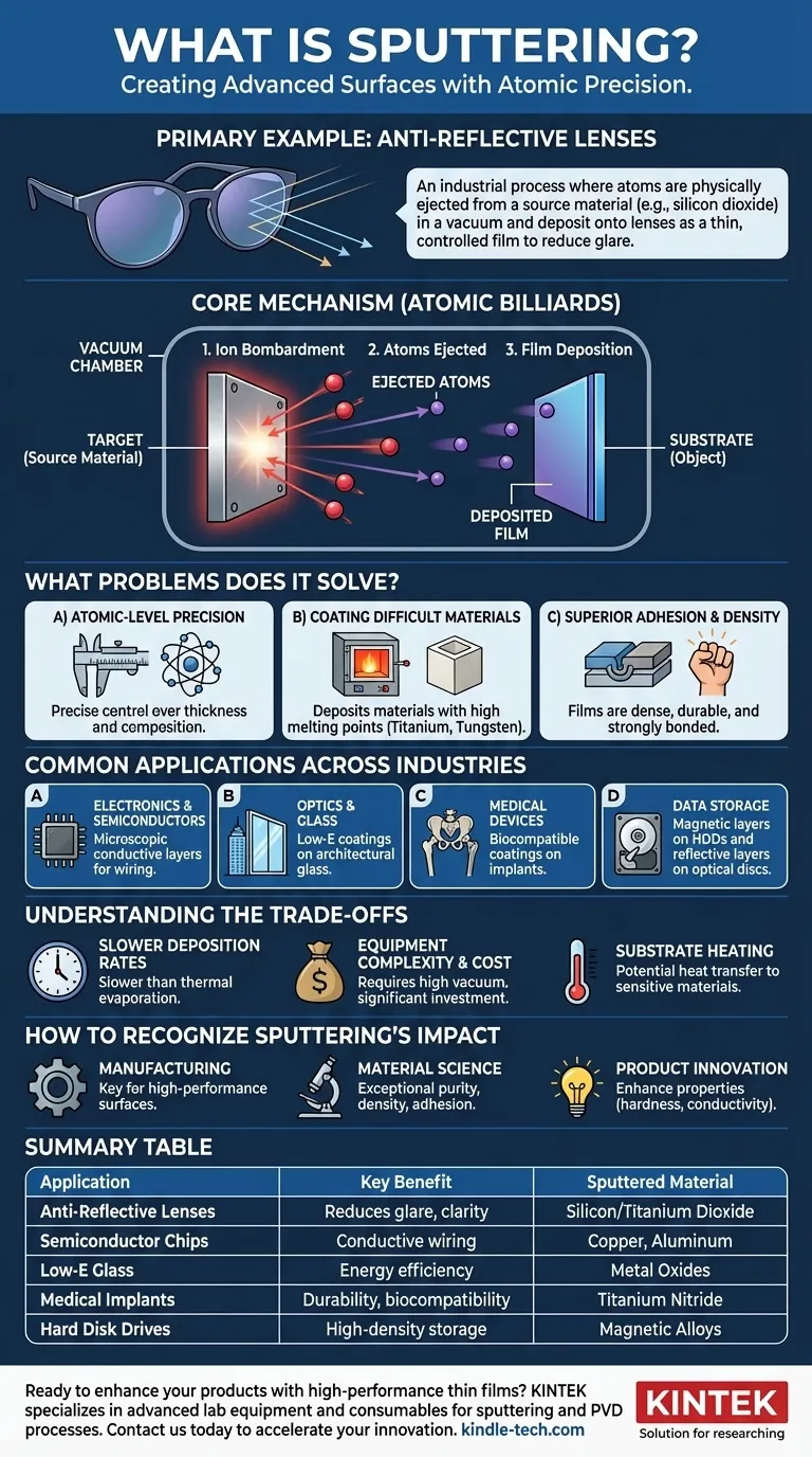
A primary example of sputtering is the creation of anti-reflective coatings on eyeglass lenses. In this industrial process, lenses are placed in a vacuum chamber where atoms are physically ejected from a source material (like silicon dioxide or titanium dioxide) by high-energy particle bombardment. These ejected atoms then travel and deposit onto the lenses as an incredibly thin, precisely controlled film, manipulating light to reduce glare and improve clarity.
Sputtering is not a single product but a foundational manufacturing technique. Its core purpose is to deposit exceptionally thin, uniform, and high-purity layers of one material onto another, enabling the creation of advanced surfaces with specialized properties that would otherwise be impossible.

What Problem Does Sputtering Solve?
Sputtering is a form of Physical Vapor Deposition (PVD). It addresses the need to create ultra-thin films with extremely high quality and control, which chemical processes or simple painting cannot achieve.
Achieving Atomic-Level Precision
The sputtering process is mechanical at the atomic level, often described as a game of "atomic billiards." Energized ions strike a source material (the "target"), knocking atoms loose.
These freed atoms travel through the vacuum and land on the object being coated (the "substrate"). This physical mechanism allows for precise control over the thickness and composition of the deposited film.
Coating with Difficult Materials
Sputtering excels at depositing materials with very high melting points, such as titanium, tungsten, or various ceramics. These materials are nearly impossible to deposit using other methods like thermal evaporation, which relies on boiling the source material.
Superior Adhesion and Density
Because the sputtered atoms arrive at the substrate with significant kinetic energy, they embed themselves slightly into the surface. This results in a film that is extremely dense, durable, and strongly bonded to the underlying material.
Common Applications Across Industries
Once you understand the core principle, you begin to see sputtering's impact across countless advanced technologies.
Electronics and Semiconductors
Sputtering is critical for manufacturing integrated circuits (computer chips). It is used to deposit the microscopic layers of conductive metals (like copper or aluminum) that form the wiring between transistors.
Optics and Glass
Beyond eyeglasses, sputtering is used to create high-performance coatings on architectural glass. These "low-emissivity" coatings reflect infrared heat, making buildings dramatically more energy-efficient without changing the look of the glass.
Medical Devices
Biocompatible coatings are applied to medical implants, such as artificial joints or pacemakers, using sputtering. These coatings, often made of titanium nitride, improve durability and reduce the chance of the body rejecting the implant.
Data Storage
The magnetic layers on traditional hard disk drives (HDDs) and the reflective layers on CDs, DVDs, and Blu-ray discs were all deposited using sputtering. The process allows for the creation of complex, multi-layered films necessary for high-density data storage.
Understanding the Trade-offs
While powerful, sputtering is a specific tool chosen for its unique advantages. It's important to understand its limitations.
Slower Deposition Rates
Compared to some other methods like thermal evaporation, sputtering can be a slower process. This is the trade-off for achieving higher film quality, density, and adhesion.
Equipment Complexity and Cost
Sputtering systems require a high vacuum, powerful energy sources, and sophisticated controls to function. This makes the initial investment in equipment significant.
Potential for Substrate Heating
The constant bombardment of high-energy particles can transfer heat to the substrate being coated. This can be a problem for heat-sensitive materials like plastics, which is why specialized variants like pulsed DC or HiPIMS sputtering were developed to manage this thermal load.
How to Recognize Sputtering's Impact
Understanding sputtering reframes how you view the surfaces of modern products. It is the enabling technology behind many material properties we take for granted.
- If your primary focus is on modern manufacturing: View sputtering as a key tool for creating high-performance surfaces, essential for everything from microchips to advanced optics.
- If your primary focus is on material science: Consider sputtering when your goal is a coating with exceptional purity, density, and adhesion, especially with complex or high-temperature materials.
- If your primary focus is on product innovation: Ask if a specialized, sputtered thin film could fundamentally enhance your product's properties, such as its hardness, conductivity, or optical performance.
Ultimately, sputtering is the invisible engineering that creates many of the most advanced and reliable material surfaces in the world.
Summary Table:
| Application | Key Benefit | Sputtered Material |
|---|---|---|
| Anti-Reflective Lenses | Reduces glare, improves clarity | Silicon Dioxide, Titanium Dioxide |
| Semiconductor Chips | Deposits microscopic conductive wiring | Copper, Aluminum |
| Low-E Glass | Reflects infrared heat for energy efficiency | Metal Oxides |
| Medical Implants | Enhances durability and biocompatibility | Titanium Nitride |
| Hard Disk Drives | Enables high-density magnetic data storage | Magnetic Alloys |
Ready to enhance your products with high-performance thin films?
KINTEK specializes in advanced lab equipment and consumables for sputtering and other Physical Vapor Deposition (PVD) processes. Whether you're developing cutting-edge optics, semiconductors, or medical devices, our solutions deliver the precision, purity, and durability your laboratory demands.
Contact us today to discuss how our expertise can accelerate your innovation and achieve superior coating results.
Visual Guide
Related Products
- Spark Plasma Sintering Furnace SPS Furnace
- Lab Sterile Slapping Type Homogenizer for Tissue Mashing and Dispersing
People Also Ask
- What technical advantages does a Spark Plasma Sintering (SPS) furnace offer for LZP ceramics? Enhance Ionic Conductivity
- Why are Spark Plasma Sintering (SPS) furnaces or hot presses utilized in the preparation of Li3PS4 solid electrolytes?
- What are the fundamentals of spark plasma sintering process? Unlock Rapid, High-Performance Material Consolidation
- What is the theory of spark plasma sintering? A Guide to Rapid, Low-Temperature Densification
- What is SPS sintering method? A Guide to High-Speed, High-Performance Material Fabrication

