At its core, DC reactive sputtering is a vacuum deposition technique used to create very thin films of compound materials. Unlike standard sputtering which deposits a pure material, this method introduces a reactive gas (like oxygen or nitrogen) into the process. This gas chemically reacts with the sputtered metal atoms, forming a new compound material, such as an oxide or nitride, directly on the surface of a substrate.
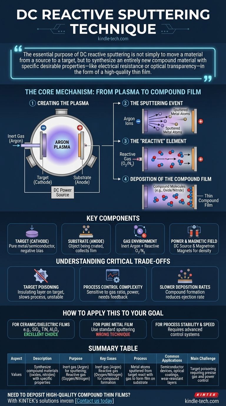
The essential purpose of DC reactive sputtering is not simply to move a material from a source to a target, but to synthesize an entirely new compound material with specific desirable properties—like electrical resistance or optical transparency—in the form of a high-quality thin film.
The Core Mechanism: From Plasma to Compound Film
To understand reactive sputtering, it's best to break it down into a sequence of events that happen inside a vacuum chamber. Each step builds on the last to create the final compound film.
Step 1: Creating the Plasma
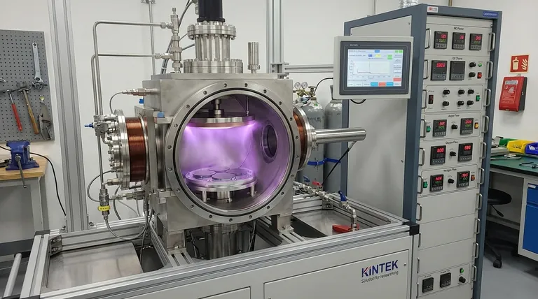
The process begins by placing a substrate (the object to be coated) and a target (the source material, like pure silicon or titanium) into a vacuum chamber. The chamber is then backfilled with a small amount of an inert gas, almost always argon. A strong Direct Current (DC) voltage is applied, making the target a negative cathode and the substrate holder a positive anode. This high voltage strips electrons from the argon atoms, creating a glowing, ionized gas known as a plasma.
Step 2: The Sputtering Event
The positively charged argon ions in the plasma are powerfully accelerated toward the negatively charged target. They bombard the target's surface with significant energy. This high-energy impact physically knocks out, or "sputters," individual atoms from the target material, launching them into the vacuum chamber.
Step 3: The "Reactive" Element
This is the defining step of the technique. A carefully controlled amount of a reactive gas, such as oxygen or nitrogen, is also introduced into the chamber. As the sputtered metal atoms travel from the target toward the substrate, they interact and chemically bond with these reactive gas molecules.
Step 4: Deposition of the Compound Film
This chemical reaction forms a new compound molecule (e.g., titanium nitride or silicon dioxide). These newly formed molecules continue their journey to the substrate, where they land and condense. Over time, this process builds up a thin, uniform, and dense layer of the compound film on the substrate's surface.
Key Components of a Reactive Sputtering System
Every DC reactive sputtering system relies on a few critical components working in concert to achieve a stable and repeatable process.
The Target (Cathode)
This is the source of the primary material and is made of a pure metal or semiconductor (e.g., Tantalum, Aluminum, Silicon). It is negatively biased to attract the positive ions from the plasma.
The Substrate (Anode)
This is the object being coated, such as a silicon wafer, glass slide, or optical component. It is typically placed on the grounded anode, where it collects the newly formed compound material.
The Gas Environment
The system uses two types of gas. An inert gas (argon) is the primary driver of the sputtering process, creating the plasma and bombarding the target. The reactive gas (oxygen, nitrogen) is the active ingredient that creates the final compound material.
The Power and Magnetic Field
A DC power source provides the stable voltage needed to create and sustain the plasma. Most modern systems are "magnetron" systems, which use strong magnets behind the target. These magnets trap electrons near the target surface, dramatically increasing the plasma's density and allowing the process to run at lower pressures and higher speeds.
Understanding the Critical Trade-offs
While powerful, DC reactive sputtering is a complex process with inherent challenges that require careful management.
Target Poisoning
The most common pitfall is target poisoning. This occurs when the reactive gas reacts not just with the sputtered atoms, but with the surface of the target itself. This forms an insulating layer on the target, which can dramatically slow down the sputtering rate, cause electrical arcing, and make the process highly unstable.
Process Control Complexity
The final film properties are extremely sensitive to the precise ratio of inert gas, reactive gas, and sputtering power. Achieving the desired chemical composition (stoichiometry) requires sophisticated feedback systems to maintain a stable balance between the metal sputtering rate and the availability of reactive gas.
Slower Deposition Rates
Generally, reactive sputtering is slower than sputtering a pure metal target. The formation of the compound on the target surface, even in a controlled state, can reduce the number of atoms ejected per incoming ion, extending process times.
How to Apply This to Your Goal
Choosing a deposition technique depends entirely on the material you need to create.
- If your primary focus is creating high-quality ceramic or dielectric films: DC reactive sputtering is an excellent choice. It is widely used for producing films like silicon dioxide (SiO₂), titanium nitride (TiN), and aluminum oxide (Al₂O₃) for semiconductor and optical applications.
- If your primary focus is depositing a pure metal film: This is the wrong technique. You should use standard (non-reactive) DC or RF sputtering with only an inert gas like argon.
- If your primary focus is process stability and speed: You must invest in advanced process control, such as optical emission monitoring or plasma impedance feedback, to manage the reactive gas flow and avoid target poisoning.
Ultimately, DC reactive sputtering offers a powerful method for engineering high-performance compound materials directly onto a surface, atom by atom.
Summary Table:
| Aspect | Description |
|---|---|
| Purpose | Synthesize compound materials (oxides, nitrides) with specific properties |
| Key Gases | Inert gas (Argon) for sputtering; Reactive gas (Oxygen/Nitrogen) for compound formation |
| Process | Metal atoms sputtered from target react with gas to form film on substrate |
| Common Applications | Semiconductor devices, optical coatings, wear-resistant layers |
| Main Challenge | Target poisoning requiring precise gas and power control |
Need to deposit high-quality compound thin films for your research or production? KINTEK specializes in lab equipment and consumables, providing reliable sputtering solutions for semiconductor, optical, and materials science applications. Our experts can help you select the right system to achieve precise film properties and stable process control. Contact us today to discuss your specific coating requirements!
Visual Guide
Related Products
- Spark Plasma Sintering Furnace SPS Furnace
- Split Chamber CVD Tube Furnace with Vacuum Station Chemical Vapor Deposition System Equipment Machine
- Customer Made Versatile CVD Tube Furnace Chemical Vapor Deposition Chamber System Equipment
- Chemical Vapor Deposition CVD Equipment System Chamber Slide PECVD Tube Furnace with Liquid Gasifier PECVD Machine
People Also Ask
- What is the difference between spark plasma sintering and flash sintering? A Guide to Advanced Sintering Methods
- What technical advantages does a Spark Plasma Sintering (SPS) furnace offer for LZP ceramics? Enhance Ionic Conductivity
- What is the process fundamentals of spark plasma sintering? Achieve Rapid, High-Density Material Consolidation
- What are the fundamentals of spark plasma sintering process? Unlock Rapid, High-Performance Material Consolidation
- What is the pressure for spark plasma sintering? A Guide to Optimizing SPS Parameters


