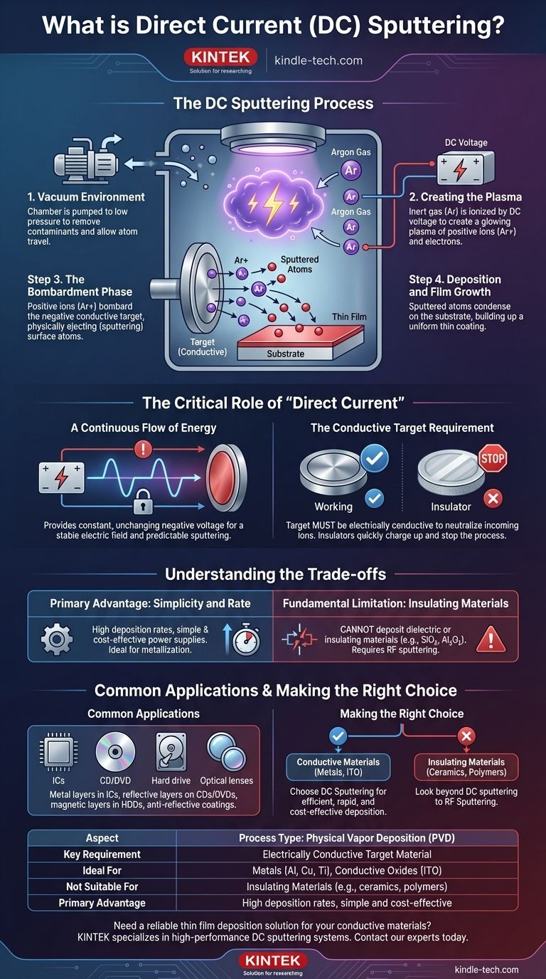
At its core, Direct Current (DC) sputtering is a physical vapor deposition (PVD) technique used to create ultra-thin films. The process uses a high DC voltage to create a plasma, which generates energetic ions that bombard a source material (the "target"). This bombardment physically knocks atoms off the target, which then travel and deposit onto a nearby substrate, forming a uniform coating.
DC sputtering is a robust and straightforward method for depositing thin films of electrically conductive materials. Its reliance on direct current, however, makes it fundamentally unsuitable for depositing insulating materials, which is its single most important limitation.
Deconstructing the DC Sputtering Process
To understand DC sputtering, it's best to visualize it as a precise, atomic-level sandblasting process happening inside a vacuum. Each step is critical for producing a high-quality film.
The Vacuum Environment
All sputtering occurs within a vacuum chamber pumped down to a very low pressure. This serves two purposes: it removes unwanted atoms like oxygen and water vapor that could contaminate the film, and it allows the sputtered atoms to travel freely from the target to the substrate.
Creating the Plasma
Once under vacuum, a small amount of an inert gas—typically argon—is introduced. A high negative DC voltage is then applied to the target material. This strong electric field energizes the argon gas, stripping electrons from the argon atoms and creating a glowing plasma composed of positive argon ions (Ar+) and free electrons.
The Bombardment Phase
The target acts as the cathode (negative electrode) in this system. The positively charged argon ions are forcefully accelerated by the electric field and slam into the negatively charged target. This collision has enough energy to physically eject, or "sputter," atoms from the target's surface.
Deposition and Film Growth
The ejected target atoms travel through the low-pressure chamber until they strike the substrate, which is strategically placed nearby. Upon arrival, these atoms condense and gradually build up on the substrate's surface, forming a thin, solid film that can be anywhere from a few nanometers to several micrometers thick.
The Critical Role of "Direct Current"
The "DC" in DC sputtering is the defining characteristic and the source of both its primary strength and its greatest weakness.
A Continuous Flow of Energy
The direct current provides a constant, unchanging negative voltage to the target. This creates a stable electric field that continuously accelerates positive ions toward the target, resulting in a steady and predictable sputtering rate.
The Conductive Target Requirement
For this process to work, the target material must be electrically conductive. As positive argon ions strike the target and are neutralized, the target must be able to replenish the lost electrons through the DC power supply. If the target were an insulator, positive charge would quickly build up on its surface, repelling the incoming argon ions and extinguishing the plasma, effectively stopping the sputtering process.
Understanding the Trade-offs
No single process is perfect for every application. The choice to use DC sputtering is governed by a clear set of advantages and limitations.
The Primary Advantage: Simplicity and Rate
For depositing metals and other conductive materials, DC sputtering is highly effective. The power supplies are relatively simple and inexpensive, and the deposition rates are generally higher than more complex sputtering techniques. This makes it a go-to process for metallization in industries like semiconductor manufacturing and optics.
The Fundamental Limitation: Insulating Materials
As explained, DC sputtering cannot be used to deposit dielectric or insulating materials like silicon dioxide (SiO₂) or aluminum oxide (Al₂O₃). The inability to conduct away the positive charge buildup on the target surface is a hard stop. For these materials, alternative techniques like Radio Frequency (RF) sputtering are required.
Common Applications
You will find DC sputtered films in a vast range of products. This includes the metal layers in integrated circuits, the reflective layers on CDs and DVDs, magnetic layers in hard disk drives, and anti-reflective or conductive coatings on optical glass.
Making the Right Choice for Your Goal
Selecting the correct deposition method comes down to the electrical properties of the material you intend to deposit.
- If your primary focus is depositing conductive materials (e.g., metals like aluminum, copper, or titanium; or conductive oxides like ITO): DC sputtering is your most efficient, rapid, and cost-effective choice.
- If your primary focus is depositing insulating materials (e.g., ceramics, polymers, or dielectrics like silicon nitride): You must look beyond DC sputtering to an alternative like RF sputtering, which is designed to overcome the charge-up problem.
Understanding this fundamental distinction between conductive and insulating targets is the key to selecting the correct deposition process for your material.
Summary Table:
| Aspect | Description |
|---|---|
| Process Type | Physical Vapor Deposition (PVD) |
| Key Requirement | Electrically Conductive Target Material |
| Ideal For | Metals (Al, Cu, Ti), Conductive Oxides (ITO) |
| Not Suitable For | Insulating Materials (e.g., ceramics, polymers) |
| Primary Advantage | High deposition rates, simple and cost-effective |
Need a reliable thin film deposition solution for your conductive materials?
KINTEK specializes in high-performance lab equipment, including DC sputtering systems designed for precision and efficiency. Whether you're working in semiconductor fabrication, optics, or materials research, our expertise ensures you get the right tool for your specific conductive coating needs.
Contact our experts today to discuss how our DC sputtering technology can enhance your laboratory's capabilities and accelerate your research and development.
Visual Guide
Related Products
- Spark Plasma Sintering Furnace SPS Furnace
- Multi Heating Zones CVD Tube Furnace Machine Chemical Vapor Deposition Chamber System Equipment
- Circulating Water Vacuum Pump for Laboratory and Industrial Use
- Vacuum Induction Melting Spinning System Arc Melting Furnace
People Also Ask
- What is the process fundamentals of spark plasma sintering? Achieve Rapid, High-Density Material Consolidation
- What are the advantages of CAMI/SPS for W-Cu composite preparation? Reduce cycles from hours to seconds.
- Why are Spark Plasma Sintering (SPS) furnaces or hot presses utilized in the preparation of Li3PS4 solid electrolytes?
- What is the pressure for spark plasma sintering? A Guide to Optimizing SPS Parameters
- What is SPS sintering method? A Guide to High-Speed, High-Performance Material Fabrication


