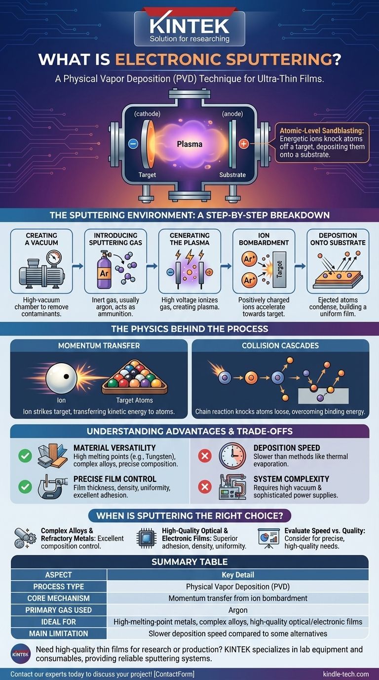
At its core, sputtering is a physical vapor deposition (PVD) technique used to create ultra-thin films with exceptional precision. The process uses energetic ions from a plasma to physically knock atoms off a source material, known as a target. These dislodged atoms then travel through a vacuum and deposit onto a substrate, gradually building a uniform coating.
Sputtering is best understood as a microscopic, atomic-level sandblasting process. Instead of using sand to erode a surface, it uses ions to chip away individual atoms from a material, which are then redeposited to form a new, highly controlled thin film on a different surface.
The Sputtering Environment: A Step-by-Step Breakdown
To understand how sputtering works, it's essential to visualize the controlled environment and sequence of events that take place inside the deposition chamber.
Step 1: Creating a Vacuum
The entire process occurs within a high-vacuum chamber. This removes air and other contaminants that could react with the sputtered atoms or interfere with their path to the substrate.
Step 2: Introducing the Sputtering Gas
A small, controlled amount of an inert gas, most commonly argon, is introduced into the chamber. This gas is not part of the final film; it simply serves as the "ammunition" for the process.
Step 3: Generating the Plasma
A strong electric field is applied within the chamber, with the source material (target) acting as the negative cathode and the object to be coated (substrate) often acting as the positive anode. This high voltage ionizes the argon gas, stripping electrons from the atoms and creating a glowing, electrically charged gas called a plasma.
Step 4: Ion Bombardment
The positively charged argon ions are forcefully accelerated by the electric field, causing them to collide with the negatively charged target material at high speeds.
Step 5: Deposition onto the Substrate
The force of these collisions is sufficient to knock atoms loose from the target's surface. These ejected atoms travel through the vacuum chamber and land on the substrate, where they condense and build up layer by layer into a thin film.
The Physics Behind the Process
Sputtering is governed by fundamental principles of physics rather than chemical reactions, which is key to its versatility and precision.
Momentum Transfer
The core mechanism is momentum transfer. When a high-energy argon ion strikes the target, it transfers its kinetic energy to the atoms within the target material, much like a cue ball striking a rack of billiard balls.
Collision Cascades
A single ion impact sets off a chain reaction, or collision cascade, within the target's atomic structure. Atoms are knocked into other atoms, transferring energy deeper into the material.
Overcoming Surface Binding Energy
For an atom to be ejected from the target, the energy it receives from the collision cascade must be greater than the surface binding energy—the force that holds it to the bulk material. If the energy is sufficient, the atom is "sputtered" away.
Understanding the Advantages and Trade-offs
Like any technical process, sputtering has distinct strengths and weaknesses that make it suitable for specific applications.
Advantage: Material Versatility
Sputtering is exceptionally effective for depositing materials with very high melting points (like tungsten or tantalum) and complex alloys. Because it's a physical process, it can deposit alloy films that retain the exact composition of the target material, which is difficult or impossible with evaporation methods.
Advantage: Precise Film Control
The technique offers precise control over film thickness, density, and uniformity. The resulting films typically exhibit excellent adhesion to the substrate due to the higher kinetic energy of the arriving atoms.
Limitation: Deposition Speed
Sputtering is generally a slower deposition process compared to other techniques like thermal evaporation. This can make it less cost-effective for applications requiring very thick films or high throughput.
Limitation: System Complexity
Sputtering systems require a high-vacuum environment and sophisticated power supplies to generate and sustain the plasma. This makes the equipment more complex and expensive than some alternative coating methods.
When is Sputtering the Right Choice?
Choosing a deposition method depends entirely on the material properties and performance required for the final product.
- If your primary focus is depositing complex alloys or refractory metals: Sputtering provides excellent control over the film's chemical composition, ensuring it matches the source material.
- If your primary focus is creating high-quality optical or electronic films: The process offers superior adhesion, density, and uniformity, which are critical for performance in microelectronics and optics.
- If your primary focus is simple, high-speed metal coating: You may want to evaluate sputtering against faster methods like thermal evaporation, weighing the trade-off between speed and ultimate film quality.
Ultimately, sputtering is a cornerstone technology that enables the manufacturing of countless modern devices, from semiconductor chips to advanced optical lenses.
Summary Table:
| Aspect | Key Detail |
|---|---|
| Process Type | Physical Vapor Deposition (PVD) |
| Core Mechanism | Momentum transfer from ion bombardment |
| Primary Gas Used | Argon |
| Ideal For | High-melting-point metals, complex alloys, high-quality optical/electronic films |
| Main Limitation | Slower deposition speed compared to some alternatives |
Need to deposit high-quality thin films for your research or production? KINTEK specializes in lab equipment and consumables, providing reliable sputtering systems and expert support to meet your specific laboratory needs. Achieve precise, uniform coatings for your most demanding applications. Contact our experts today to discuss your project!
Visual Guide
Related Products
- Single Punch Electric Tablet Press Machine TDP Tablet Punching Machine
- Laboratory Scientific Electric Heating Blast Drying Oven
- Electron Beam Evaporation Coating Oxygen-Free Copper Crucible and Evaporation Boat
- Three-dimensional electromagnetic sieving instrument
- Spark Plasma Sintering Furnace SPS Furnace
People Also Ask
- What are the different parts of a single punch tablet machine? The Core Components Explained
- What are the two classifications of press machines? Single Punch vs. Rotary Presses Explained
- What is the use of single punch tablet press? For Precise R&D and Small-Batch Tablet Production
- What is a tablet punching machine called? Choosing the Right Press for Your Production Scale
- What is a single punch tablet machine? The Essential Tool for Lab-Scale Tablet R&D


