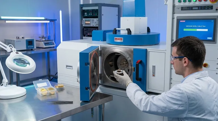
In scanning electron microscopy, sputter coating is a fundamental sample preparation technique for non-conductive specimens. It involves depositing an ultra-thin layer of a conductive metal, such as gold or platinum, onto the sample's surface. This coating, typically only 5-10 nanometers thick, prevents electrical charge from building up when the sample is scanned by the electron beam, which is the primary cause of poor image quality and artifacts.
Sputter coating solves the critical problem of "sample charging" in non-conductive materials. While it dramatically improves image quality and stability, it is a deliberate trade-off that conceals the sample's true elemental composition beneath a metallic film.
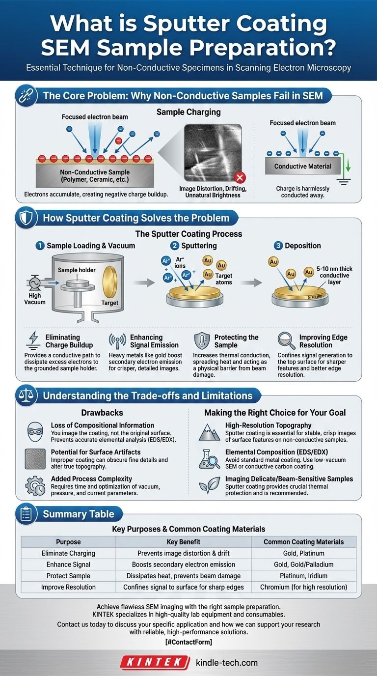
The Core Problem: Why Non-Conductive Samples Fail in SEM
To understand the value of sputter coating, you must first understand the problem it solves. Scanning electron microscopes (SEMs) work by bombarding a sample with a focused beam of electrons.
What is Sample Charging?
When the electron beam hits a conductive material, any excess electrical charge is harmlessly conducted away to the ground.
However, on a non-conductive or poorly conductive sample (like a polymer, ceramic, or biological specimen), these electrons have nowhere to go. They accumulate on or near the surface, creating a negative charge buildup. This phenomenon is known as sample charging.
The Consequences of Charging
Sample charging is highly destructive to image quality. It can cause a range of severe artifacts, including image distortion, unnatural brightness in certain areas, and erratic shifting or drifting of the image as you try to focus. In essence, the accumulated charge deflects the incoming electron beam and interferes with the detector's ability to collect a clean signal.
How Sputter Coating Solves the Problem
Applying a thin, conductive coating provides a path for electrical charge to dissipate, effectively turning a non-conductive sample into a conductive one from the electron beam's perspective.
Eliminating Charge Buildup
This is the primary benefit. The conductive layer is connected to the SEM sample holder (which is grounded), creating a path for excess electrons to flow away from the surface. This stabilizes the imaging process and eliminates the distortions caused by charging.
Enhancing Signal Emission
High-quality SEM images are most often formed using secondary electrons—low-energy electrons ejected from the sample's surface atoms. Heavy metals used for coating, like gold, are very efficient at emitting secondary electrons. This boosts the signal-to-noise ratio, resulting in a crisper, more detailed image.
Protecting the Sample
The electron beam deposits a significant amount of energy into the sample, which can cause damage, especially to delicate biological or polymeric materials. The metal coating helps by increasing thermal conduction, spreading the heat out and preventing localized damage. It also acts as a physical barrier.
Improving Edge Resolution
By preventing the primary electron beam from penetrating deep into the low-density sample, the coating ensures that the signal is generated only from the very top surface. This confinement of the interaction volume leads to sharper-looking features and better edge resolution.
Understanding the Trade-offs and Limitations
Sputter coating is a powerful tool, but it is not a perfect solution. An expert user must be aware of its inherent compromises.
Loss of Compositional Information
The most significant drawback is that you are no longer imaging the actual sample surface. You are imaging the metal coating. This means you lose all atomic number contrast and cannot perform accurate elemental analysis (like EDS/EDX) on the original surface, as the detector will primarily see the coating material.
Potential for Surface Artifacts
While the goal is a uniform coating, improper technique can introduce artifacts. If the coating is too thick, it can obscure very fine surface details and alter the sample's true topography.
Added Process Complexity
Sputter coating is an additional step that requires time and careful optimization. Parameters like vacuum level, gas pressure, current, and coating time must be controlled to achieve a good result without damaging the sample or creating an overly thick layer.
Making the Right Choice for Your Goal
Deciding whether to coat your sample depends entirely on what information you need to extract from it.
- If your primary focus is high-resolution surface topography: Sputter coating is almost always the correct choice for a non-conductive sample. It is the most reliable way to get a stable, crisp image of surface features.
- If your primary focus is elemental composition (EDS/EDX): Do not use a standard metal sputter coater. This will completely invalidate your results. Consider using a low-vacuum SEM (if available) or applying a conductive carbon coating, which produces less interference.
- If your primary focus is imaging a delicate, beam-sensitive sample: Sputter coating provides crucial protection from thermal damage and is highly recommended.
Ultimately, effective SEM work relies on choosing the right preparation technique to answer your specific scientific question.
Summary Table:
| Purpose | Key Benefit | Common Coating Materials |
|---|---|---|
| Eliminate Charging | Prevents image distortion & drift | Gold, Platinum |
| Enhance Signal | Boosts secondary electron emission | Gold, Gold/Palladium |
| Protect Sample | Dissipates heat, prevents beam damage | Platinum, Iridium |
| Improve Resolution | Confines signal to surface for sharp edges | Chromium (for high resolution) |
Achieve flawless SEM imaging with the right sample preparation.
Sputter coating is essential for obtaining clear, stable images from non-conductive materials. Choosing the correct equipment and parameters is critical to avoid artifacts and protect your samples.
KINTEK specializes in high-quality lab equipment and consumables for all your laboratory needs. Our experts can help you select the ideal sputter coater and accessories to ensure your SEM analysis is a success.
Contact us today to discuss your specific application and how we can support your research with reliable, high-performance solutions.
Visual Guide
Related Products
- Custom CVD Diamond Coating for Lab Applications
- HFCVD Machine System Equipment for Drawing Die Nano-Diamond Coating
- Chemical Vapor Deposition CVD Equipment System Chamber Slide PECVD Tube Furnace with Liquid Gasifier PECVD Machine
- Multifunctional Electrolytic Electrochemical Cell Water Bath Single Layer Double Layer
- Professional Cutting Tools for Carbon Paper Cloth Diaphragm Copper Aluminum Foil and More
People Also Ask
- What are the types of CVD coating? A Guide to Choosing the Right Process
- Can you coat something in diamond? Unlock Unmatched Hardness and Thermal Conductivity
- What are the advantages of CVD coating? Superior Hardness and Uniformity for Demanding Applications
- How thick is CVD diamond coating? Balancing Durability and Stress for Optimal Performance
- What is CVD coating? Transform Your Material's Surface for Maximum Performance


