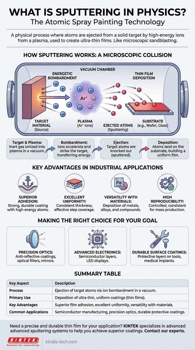
In simple terms, sputtering is a physical process where atoms are ejected from a solid target material after it is bombarded by high-energy particles, typically ions from a plasma. This microscopic-scale "sandblasting" effect occurs naturally in space but is more widely known as a highly controlled industrial technique for creating or removing ultra-thin films.
Sputtering is best understood as a versatile "atomic spray painting" technology. It leverages physical momentum to precisely transfer material from a source target onto a substrate, resulting in exceptionally uniform and durable coatings for high-tech applications.
How Sputtering Works: A Microscopic Collision
At its core, sputtering is a process of momentum transfer, a key technique within a broader category called Physical Vapor Deposition (PVD). It doesn't rely on chemical reactions or melting; it is a purely physical phenomenon.
The Target Material
The process begins with a "target," which is a piece of the solid material you wish to deposit as a thin film. This could be a metal, an alloy, or a ceramic compound.
The Energetic Bombardment
This target is placed in a vacuum chamber filled with an inert gas, such as argon. A strong electric field is applied, which ignites the gas into a plasma—a state of matter containing positively charged ions and free electrons.
The Ejection of Atoms
These positively charged gas ions are accelerated by the electric field and smash into the negatively charged target surface. When an ion collides with the target, it transfers its kinetic energy, knocking out or "sputtering" microscopic particles from the target material.
Thin Film Deposition
These ejected atoms travel through the vacuum chamber and land on another surface, known as the substrate (e.g., a silicon wafer, a piece of glass, or a medical implant). Over time, these atoms build up on the substrate, forming a dense, uniform, and extremely thin film.
Key Advantages in Industrial Applications
Sputtering is not just a scientific curiosity; it is a cornerstone of modern manufacturing because of the unique characteristics of the films it produces. The control and quality it offers make it indispensable.
Superior Film Quality
Sputtered films are known for their strong adhesion to the substrate. Because the sputtered atoms arrive with high energy, they embed themselves tightly, creating a very durable and robust coating.
Excellent Uniformity and Coverage
The process allows for excellent film thickness uniformity across large surfaces. It can also effectively coat complex, three-dimensional shapes, a property known as "step coverage," which is critical in microelectronics.
Versatility with Materials
Sputtering can be used to deposit a vast range of materials, including complex alloys and compounds. The composition of the sputtered film remains very close to the composition of the source target, allowing for precise material engineering.
High Reproducibility and Control
The process is highly controllable and reproducible, making it ideal for mass production where consistency is paramount. Parameters like power and gas pressure can be finely tuned to achieve desired film properties.
Making the Right Choice for Your Goal
Understanding the core strengths of sputtering helps clarify when it is the optimal choice over other deposition methods. Your application's primary need will determine its suitability.
- If your primary focus is precision optics: Sputtering delivers the exceptional uniformity and density required for anti-reflective coatings, optical filters, and mirrors.
- If your primary focus is advanced electronics: The technique is essential for depositing the conductive and insulating layers in semiconductor devices and LED displays.
- If your primary focus is creating durable surface coatings: Sputtering provides the strong adhesion necessary for protective layers on tools, medical implants, and other components requiring high wear resistance.
Ultimately, sputtering provides engineers with atomic-level control over surfaces, making it a foundational tool for creating modern high-technology components.
Summary Table:
| Key Aspect | Description |
|---|---|
| Process | Ejection of target atoms via ion bombardment in a vacuum. |
| Primary Use | Deposition of ultra-thin, uniform coatings (thin films). |
| Key Advantages | Superior film adhesion, excellent uniformity, versatility with materials. |
| Common Applications | Semiconductor manufacturing, precision optics, durable protective coatings. |
Need a precise and durable thin film for your application? KINTEK specializes in advanced lab equipment, including sputtering systems, to help you achieve superior coatings for semiconductors, optics, and durable surfaces. Contact our experts today to discuss how our solutions can enhance your laboratory's capabilities and product performance.
Visual Guide
Related Products
- Lab Sterile Slapping Type Homogenizer for Tissue Mashing and Dispersing
- Spark Plasma Sintering Furnace SPS Furnace
- Single Punch Manual Tablet Press Machine TDP Tablet Punching Machine
People Also Ask
- How does a homogenizer affect the quality of electrode slurry? Master Battery Consistency with High-Shear Mixing
- What is the role of an ultrasonic cleaner during magnesium alloy coating? Ensure Superior Adhesion and Surface Purity
- How does a laboratory automatic masticator or homogenizer facilitate the processing of biofilm samples? Optimize Accuracy
- What role does an ultrasonic cleaner play in the pre-treatment of 4140 steel? Ensure Uniform Nitriding Activation
- What is the primary function of an ultrasonic cleaner in coating? Achieve Unmatched Substrate Purity for PVD Adhesion


