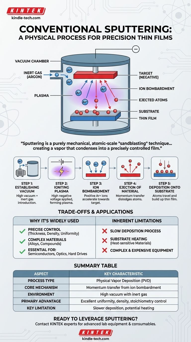
At its core, conventional sputtering is a physical process that uses high-energy ions to eject atoms from a source material, known as a target, which then deposit onto a substrate to form a highly uniform thin film. This entire process takes place within a vacuum chamber filled with an inert gas, typically Argon, to ensure the purity and control of the resulting coating.
Sputtering is not a chemical reaction or a melting process. It is a purely mechanical, atomic-scale "sandblasting" technique where an energized plasma provides the momentum to dislodge material from a target, creating a vapor that condenses into a precisely controlled film.

The Mechanics of the Sputtering Process
Sputtering is a type of Physical Vapor Deposition (PVD) that relies on a sequence of controlled physical events. Understanding each step is key to appreciating its precision.
Step 1: Establishing the Vacuum Environment
The entire process begins by placing the target material and the substrate into a sealed chamber. This chamber is pumped down to a high vacuum to remove air and other contaminants that could interfere with the process or become trapped in the film.
Once a vacuum is achieved, a small, controlled amount of an inert gas, usually Argon, is introduced.
Step 2: Igniting the Plasma
A high negative voltage is applied to the target material. This strong electric field energizes the inert Argon gas, stripping electrons from the Argon atoms.
This creates a self-sustaining plasma, a glowing state of matter consisting of positively charged Argon ions (Ar+) and free electrons.
Step 3: Ion Bombardment
The positively charged Argon ions are now forcefully accelerated by the electric field toward the negatively charged target.
They collide with the target's surface with significant kinetic energy.
Step 4: Ejection of Target Material
This high-energy impact is a momentum transfer event. The force of the collision is sufficient to physically knock out, or "sputter," atoms from the surface of the target.
These ejected particles are typically neutral atoms, not ions. They travel away from the target in a straight line.
Step 5: Deposition onto the Substrate
The sputtered atoms traverse the vacuum chamber and strike the substrate, which is strategically placed to intercept them.
Upon hitting the substrate, these atoms condense and gradually build up, layer by layer, to form a thin, dense, and highly uniform film.
Understanding the Trade-offs and Applications
Like any technical process, sputtering has distinct advantages and limitations that make it suitable for specific applications.
Why Sputtering is Widely Used
The primary strength of sputtering is its control and versatility. It allows for precise management of film thickness, density, and uniformity.
Because it physically transfers material, it's excellent for depositing complex materials like alloys or compounds while preserving their original chemical composition. This makes it essential in manufacturing semiconductors, optical coatings, hard drives, and other high-performance electronic components.
Inherent Limitations of the Conventional Method
Conventional sputtering can be a relatively slow deposition process compared to other methods like thermal evaporation.
The process also generates considerable heat at the target, which can radiate and heat the substrate. This can be a significant drawback when coating heat-sensitive materials like plastics. Furthermore, the high-vacuum equipment required is complex and expensive.
Making the Right Choice for Your Goal
The decision to use sputtering depends entirely on the required properties of the final film.
- If your primary focus is material purity and film density: Sputtering is often superior, as the high-energy deposition results in dense, well-adhered films with fewer impurities than many other methods.
- If your primary focus is coating complex alloys or compounds: Sputtering excels because it generally preserves the stoichiometry (the elemental ratio) of the target material in the final film.
- If your primary focus is coating large areas with simple metals quickly: You may find that other PVD methods, such as thermal evaporation, offer a more cost-effective and faster solution.
Ultimately, understanding sputtering as a controlled, momentum-transfer process empowers you to leverage its precision for creating high-performance thin films.
Summary Table:
| Aspect | Key Characteristic |
|---|---|
| Process Type | Physical Vapor Deposition (PVD) |
| Core Mechanism | Momentum transfer from ion bombardment |
| Environment | High vacuum with inert gas (e.g., Argon) |
| Primary Advantage | Excellent film uniformity, density, and stoichiometry control |
| Key Limitation | Slower deposition rate and potential substrate heating |
Ready to leverage sputtering for your high-performance thin films?
At KINTEK, we specialize in providing advanced lab equipment and consumables for precise material deposition. Whether you're developing semiconductors, optical coatings, or other electronic components, our solutions ensure the material purity and film density you require.
Contact our experts today to discuss how our sputtering systems can meet your specific laboratory needs and enhance your research and production capabilities.
Visual Guide
Related Products
- Spark Plasma Sintering Furnace SPS Furnace
- Vacuum Induction Melting Spinning System Arc Melting Furnace
- Chemical Vapor Deposition CVD Equipment System Chamber Slide PECVD Tube Furnace with Liquid Gasifier PECVD Machine
- Customer Made Versatile CVD Tube Furnace Chemical Vapor Deposition Chamber System Equipment
People Also Ask
- What is the theory of spark plasma sintering? A Guide to Rapid, Low-Temperature Densification
- What technical advantages does a Spark Plasma Sintering (SPS) furnace offer for LZP ceramics? Enhance Ionic Conductivity
- Why are Spark Plasma Sintering (SPS) furnaces or hot presses utilized in the preparation of Li3PS4 solid electrolytes?
- What is SPS sintering method? A Guide to High-Speed, High-Performance Material Fabrication
- What is the mechanism of SPS process? A Deep Dive into Rapid, Low-Temperature Sintering


