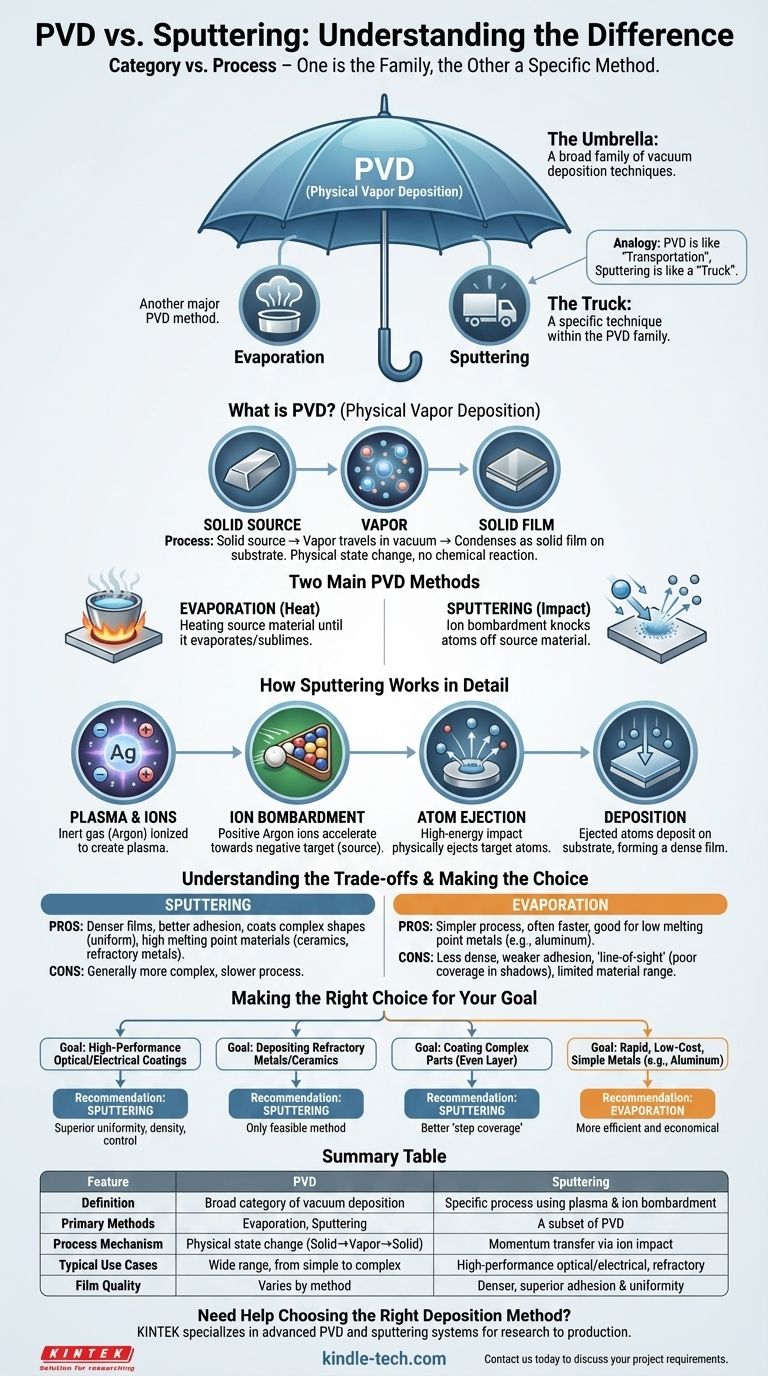
The fundamental difference is one of category versus process. Sputtering is a specific technique used to create a thin film, whereas Physical Vapor Deposition (PVD) is the broad family of techniques that includes sputtering, as well as other methods like thermal and e-beam evaporation. Think of PVD as "transportation" and sputtering as a "truck"—a truck is a type of transportation, but not all transportation is a truck.
The core misconception is viewing PVD and sputtering as competing alternatives. In reality, sputtering is one of the two major methods that fall under the umbrella of PVD. Understanding this hierarchy is the key to grasping how modern thin-film coatings are made.
What is Physical Vapor Deposition (PVD)?
PVD describes a variety of vacuum deposition methods that use purely physical means to transfer a material from a source to a substrate.
The Core Principle of PVD
All PVD processes occur in a vacuum and share a common sequence: a solid source material is converted into a vapor, this vapor travels across the chamber, and it then condenses onto a substrate as a solid, thin film. The "physical" part of the name means the material changes its state—from solid to vapor and back to solid—without undergoing a chemical reaction.
The Two Main PVD Methods
PVD is broadly divided into two major approaches based on how the material is turned into a vapor: evaporation and sputtering.
-
Evaporation: This method involves heating the source material until it evaporates or sublimes. Think of it like boiling water, where the resulting steam (vapor) condenses on a cold surface.
-
Sputtering: This method uses ion bombardment to physically knock atoms off the source material. Imagine a cue ball breaking a rack of billiard balls—the high-energy impact sends particles scattering.
How Sputtering Works in Detail
Sputtering is a highly controlled and versatile PVD process that relies on momentum transfer rather than heat.
The Role of Plasma
First, an inert gas—typically Argon—is introduced into the vacuum chamber. An electric field is applied, which ionizes the gas and creates a glowing plasma.
The Bombardment Process
The source material, known as the "target," is given a negative electrical charge. This causes the positive ions from the plasma (Argon ions) to accelerate and collide with the target at high speed.
Atom Ejection and Deposition
Each collision has enough energy to physically "sputter" or eject atoms from the target's surface. These ejected atoms travel through the vacuum chamber and deposit onto the substrate, gradually building a dense and uniform thin film.
Understanding the Trade-offs: Sputtering vs. Evaporation
While both are PVD processes, choosing between sputtering and evaporation depends entirely on the material and the desired properties of the final film.
Film Density and Adhesion
Sputtering produces films that are generally denser and adhere more strongly to the substrate. The sputtered atoms arrive with higher kinetic energy, embedding them more firmly onto the surface.
Material Compatibility
Sputtering is exceptionally versatile. It can deposit materials with extremely high melting points, such as ceramics and refractory metals, which are impossible to deposit using evaporation.
Deposition Control and Uniformity
Sputtering offers superior control over film thickness and can more easily coat complex, three-dimensional shapes with a uniform layer. Evaporation tends to be more of a "line-of-sight" process, making it difficult to coat shadowed areas.
Process Speed and Complexity
Evaporation can often be a faster and simpler process for certain materials, especially those with lower melting points like aluminum. Sputtering systems are typically more complex.
Making the Right Choice for Your Goal
Selecting the correct PVD method requires matching the process capabilities to your application's needs.
- If your primary focus is high-performance optical or electrical coatings: Sputtering is almost always preferred for its superior uniformity, density, and control.
- If your primary focus is depositing refractory metals or ceramics: Sputtering is the only feasible PVD method, as these materials cannot be easily evaporated.
- If your primary focus is rapid, low-cost deposition of simple metals like aluminum: E-beam or thermal evaporation can be a more efficient and economical choice.
- If your primary focus is coating a complex part with an even layer: Sputtering provides better "step coverage" and will deliver a more uniform film than evaporation.
Ultimately, both sputtering and evaporation are powerful tools in the PVD family, each with distinct advantages for specific manufacturing challenges.
Summary Table:
| Feature | PVD (Physical Vapor Deposition) | Sputtering (A Type of PVD) |
|---|---|---|
| Definition | Broad category of vacuum deposition methods | Specific process using plasma and ion bombardment |
| Primary Methods | Evaporation, Sputtering | A subset of PVD |
| Process Mechanism | Physical state change (solid→vapor→solid) | Momentum transfer via ion impact |
| Typical Use Cases | Wide range, from simple metallization to complex coatings | High-performance optical/electrical coatings, refractory materials |
| Film Quality | Varies by method | Denser films, superior adhesion and uniformity |
Need Help Choosing the Right Deposition Method?
Understanding the nuances between PVD techniques like sputtering and evaporation is crucial for achieving optimal results in your lab. The right equipment can significantly impact film quality, adhesion, and overall project success.
KINTEK specializes in advanced lab equipment and consumables, including state-of-the-art PVD and sputtering systems. We serve a wide range of laboratory needs, from research and development to high-volume production.
Let our experts help you select the perfect solution for your specific application—whether you require the versatility of sputtering for complex coatings or the efficiency of evaporation for simpler tasks.
Contact us today to discuss your project requirements and discover how KINTEK can enhance your laboratory's capabilities!
Visual Guide
Related Products
- RF PECVD System Radio Frequency Plasma-Enhanced Chemical Vapor Deposition RF PECVD
- Split Chamber CVD Tube Furnace with Vacuum Station Chemical Vapor Deposition System Equipment Machine
- Chemical Vapor Deposition CVD Equipment System Chamber Slide PECVD Tube Furnace with Liquid Gasifier PECVD Machine
- VHP Sterilization Equipment Hydrogen Peroxide H2O2 Space Sterilizer
- Vacuum Hot Press Furnace Heated Vacuum Press Machine Tube Furnace
People Also Ask
- How are PECVD and CVD different? A Guide to Choosing the Right Thin-Film Deposition Process
- What are the applications of PECVD? Essential for Semiconductors, MEMS, and Solar Cells
- What is an example of PECVD? RF-PECVD for High-Quality Thin Film Deposition
- How does RF power create plasma? Achieve Stable, High-Density Plasma for Your Applications
- What are the benefits of PECVD? Achieve Superior Low-Temperature Thin Film Deposition