The core distinction is one of category and mechanism. Deposition is the broad, overarching term for any process that applies a thin film of material onto a surface (a substrate). Sputtering is not a separate process, but rather a specific and widely used method of deposition that falls under the category of Physical Vapor Deposition (PVD).
The confusion between "sputtering" and "deposition" arises because they are not competing processes. Instead, deposition is the overall goal of adding a thin film, while sputtering is a specific physical technique used to achieve it.
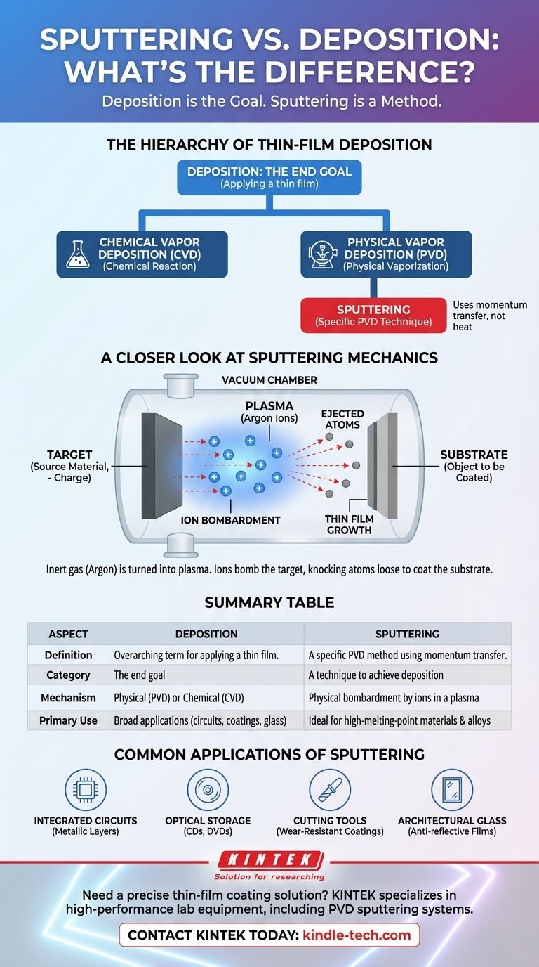
The Hierarchy of Thin-Film Deposition
To understand sputtering, you must first understand its place within the broader field of thin-film deposition. This field is primarily divided into two major families of techniques.
Deposition: The End Goal
At its most fundamental level, deposition refers to any process where atoms or molecules are transferred onto a solid surface to form a thin, solid coating. This is the desired outcome, regardless of the method used.
Applications range from applying anti-reflective coatings on glass to creating the intricate layers of a modern integrated circuit.
The Two Major Families: Physical vs. Chemical
All deposition methods fall into one of two categories based on their underlying mechanism.
-
Physical Vapor Deposition (PVD): In PVD, a solid material is converted into a vapor through physical means (like bombardment or heating) in a vacuum. This vapor then travels and condenses onto the substrate. Sputtering is a primary PVD method.
-
Chemical Vapor Deposition (CVD): In CVD, the substrate is exposed to volatile precursor chemicals. These chemicals react or decompose on the substrate's surface to produce the desired film. The process is chemical, not physical.
A Closer Look at Sputtering Mechanics
Sputtering is a highly controlled PVD technique that uses momentum transfer to create the material vapor, rather than heat.
The Role of Plasma and Inert Gas
The process begins in a vacuum chamber that is backfilled with a small amount of an inert gas, almost always argon. An electric field is applied, which ignites this gas into a plasma—a high-energy state of matter containing positively charged argon ions and free electrons.
From Target to Substrate
Inside the chamber, the source material to be deposited is known as the target. This target is given a negative electrical charge. The substrate (the object to be coated) is positioned to face the target.
The Impact of Ion Bombardment
The positively charged argon ions in the plasma are accelerated by the electric field and violently collide with the negatively charged target. This high-energy bombardment is forceful enough to physically knock atoms loose from the target material.
These ejected atoms travel through the vacuum chamber and land on the substrate, gradually building up a thin, uniform film. This ejection and subsequent coating is sputter deposition.
Understanding the Trade-offs and Applications
Sputtering is not a universal solution. Its physical mechanism provides distinct advantages but also comes with specific operational requirements.
Key Advantages of Sputtering
Sputtering excels at depositing materials with very high melting points, like carbon or silicon, which are difficult to process using heat-based evaporation methods.
It is also highly effective for depositing alloys and compounds, as the bombardment process tends to preserve the original chemical composition of the target material in the final film.
Operational Constraints
The process requires a vacuum and must operate within a specific pressure range to sustain the plasma. It is also generally a slower deposition method compared to some thermal evaporation techniques.
Furthermore, depositing insulating materials requires a more complex setup using a radio frequency (RF) power source instead of a simple DC source to prevent charge buildup on the target.
Common Industrial Applications
Sputtering is a cornerstone of modern manufacturing. It is used for:
- Creating the metallic layers in integrated circuits.
- Applying coatings on CDs and DVDs.
- Depositing wear-resistant coatings on cutting tools.
- Creating anti-reflective or high-emissivity films on architectural glass.
Selecting the Right Deposition Strategy
Choosing a method depends entirely on the material properties and the desired outcome of the film.
- If your primary focus is depositing high-melting-point materials or complex alloys: Sputtering is an ideal choice, as its physical bombardment mechanism bypasses the need for extreme heat.
- If your primary focus is creating a film through surface chemical reactions: You are likely looking at Chemical Vapor Deposition (CVD), a distinct category from the physical process of sputtering.
- If your primary focus is simply understanding the terminology: Remember that deposition is the general term for any thin-film coating process, and sputtering is one specific technique to achieve it.
Understanding this fundamental hierarchy is the first step toward navigating the world of thin-film technology.
Summary Table:
| Aspect | Deposition | Sputtering |
|---|---|---|
| Definition | Overarching term for applying a thin film to a substrate | A specific PVD method using momentum transfer |
| Category | The end goal | A technique to achieve deposition |
| Mechanism | Can be physical (PVD) or chemical (CVD) | Physical bombardment by ions in a plasma |
| Primary Use | Broad applications (circuits, coatings, glass) | Ideal for high-melting-point materials and alloys |
Need a precise thin-film coating solution for your lab?
Whether you are developing advanced materials, creating semiconductor layers, or applying specialized coatings, selecting the right deposition method is critical for your results. KINTEK specializes in high-performance lab equipment, including sputtering systems for PVD, designed to handle complex materials like alloys and high-melting-point substances with precision.
Let our experts help you choose the perfect equipment to enhance your research and development. Contact KINTEK today to discuss your specific laboratory needs and discover the ideal deposition solution for your projects.
Visual Guide