At its core, sputter deposition is a highly controlled physical process used to create exceptionally thin and uniform films of material. It functions by bombarding a solid source material, called a "target," with energetic ions inside a vacuum. These collisions physically knock atoms loose from the target, which then travel and deposit onto a component, known as the "substrate," building the desired film layer by layer.
Sputter deposition is not about melting or boiling a material; it is a mechanical process at the atomic scale. This fundamental difference—using momentum transfer instead of heat—is what gives it the unique ability to deposit a vast range of high-performance materials with exceptional precision and adhesion.
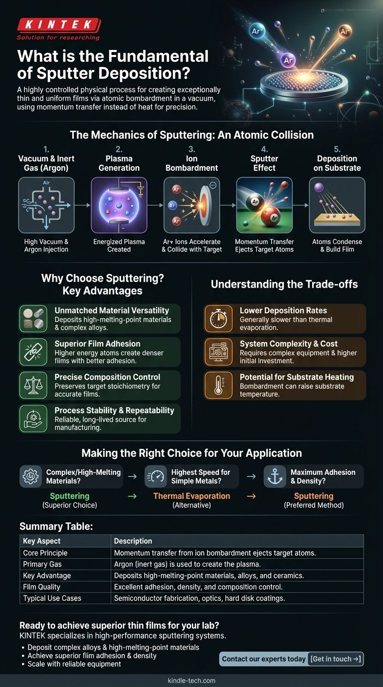
The Mechanics of Sputtering: An Atomic Collision
To grasp the fundamentals, it helps to visualize the process as a series of distinct physical events happening at the atomic level. The entire operation takes place within a sealed vacuum chamber.
### The Role of the Vacuum and Inert Gas
First, the chamber is evacuated to a high vacuum to remove air and other contaminants that could interfere with the process. A small, controlled amount of an inert gas, most commonly argon, is then introduced into the chamber.
### Generating the Plasma
A strong electric field is applied within the chamber. This field energizes the argon gas, stripping electrons from the argon atoms and creating a plasma—a glowing, ionized gas consisting of positively charged argon ions and free electrons.
### The Bombardment Process
The target material is given a negative electrical charge. This attracts the positively charged argon ions from the plasma, causing them to accelerate and collide with the target's surface at high velocity.
### The "Sputter" Effect: Momentum Transfer
This is the central principle of sputtering. When an argon ion strikes the target, it transfers its momentum to the atoms in the target material, much like a cue ball breaking a rack of billiard balls. This transfer of energy and momentum is forceful enough to eject, or "sputter," individual atoms from the target's surface.
### Deposition on the Substrate
The sputtered atoms travel in a straight line from the target until they strike a surface. By strategically placing a substrate (the part to be coated) in their path, these atoms land and condense on it, gradually building up a thin, dense, and highly uniform film.
Why Choose Sputtering? Key Advantages
The atomic collision mechanism gives sputter deposition several powerful advantages over other methods like thermal evaporation.
### Unmatched Material Versatility
Because sputtering does not rely on melting, it can be used to deposit materials with extremely high melting points, such as refractory metals and ceramics, that are difficult or impossible to evaporate. It works equally well for pure elements, complex alloys, and compounds.
### Superior Film Adhesion
Sputtered atoms are ejected with significantly more kinetic energy than evaporated atoms. This higher energy helps them embed slightly into the substrate surface, resulting in a denser film and dramatically better adhesion.
### Precise Composition Control
When sputtering an alloy target, the atoms are ejected in a way that preserves the material's original composition. This means the resulting film has a stoichiometry that is very close to that of the source target, which is critical for high-performance electronics and optics.
### Process Stability and Repeatability
The target erodes slowly and predictably, providing a stable, long-lived deposition source. This makes sputtering an extremely reliable and repeatable process, essential for high-volume manufacturing in industries like semiconductor fabrication and hard disk production.
Understanding the Trade-offs
No process is perfect. Objectivity requires acknowledging the practical limitations of sputter deposition.
### Lower Deposition Rates
Generally, sputter deposition is a slower process compared to thermal evaporation. The rate at which atoms are ejected is often lower, meaning it can take longer to build a film of a certain thickness.
### System Complexity and Cost
Sputtering systems are mechanically complex, requiring high-vacuum pumps, precise gas flow controllers, and sophisticated high-voltage power supplies. This makes the initial equipment investment higher than for simpler deposition techniques.
### Potential for Substrate Heating
While sputtering is a "non-thermal" process with low radiant heat, the constant bombardment of energetic atoms and plasma particles can cause the substrate's temperature to rise. For extremely temperature-sensitive substrates, this must be managed with a cooling system.
Making the Right Choice for Your Application
Selecting a deposition method depends entirely on your material, substrate, and the desired properties of the final film.
- If your primary focus is depositing complex alloys or high-melting-point materials: Sputtering is the superior choice due to its non-thermal nature and excellent composition control.
- If your primary focus is achieving the highest possible deposition speed for a simple metal: Thermal evaporation might be a more cost-effective and faster alternative.
- If your primary focus is ensuring maximum film adhesion and density: Sputtering is the preferred method, as the energetic atoms create a stronger bond with the substrate.
Ultimately, understanding the principle of atomic momentum transfer is the key to leveraging sputter deposition for creating advanced, high-performance surfaces.
Summary Table:
| Key Aspect | Description |
|---|---|
| Core Principle | Momentum transfer from ion bombardment ejects target atoms. |
| Primary Gas | Argon (inert gas) is used to create the plasma. |
| Key Advantage | Deposits high-melting-point materials, alloys, and ceramics. |
| Film Quality | Excellent adhesion, density, and composition control. |
| Typical Use Cases | Semiconductor fabrication, optics, hard disk coatings. |
Ready to achieve superior thin films for your lab?
Sputter deposition is ideal for applications requiring precise control over material composition and exceptional film adhesion. KINTEK specializes in high-performance lab equipment, including sputtering systems, to meet the demanding needs of research and production laboratories.
We can help you:
- Deposit complex alloys and high-melting-point materials with precision.
- Achieve superior film adhesion and density for durable coatings.
- Scale your process with reliable and repeatable equipment.
Contact our experts today to discuss how a KINTEK sputtering system can advance your projects. Get in touch →
Visual Guide
Related Products
- Chemical Vapor Deposition CVD Equipment System Chamber Slide PECVD Tube Furnace with Liquid Gasifier PECVD Machine
- HFCVD Machine System Equipment for Drawing Die Nano-Diamond Coating
- 915MHz MPCVD Diamond Machine Microwave Plasma Chemical Vapor Deposition System Reactor
- RF PECVD System Radio Frequency Plasma-Enhanced Chemical Vapor Deposition RF PECVD
- Customer Made Versatile CVD Tube Furnace Chemical Vapor Deposition Chamber System Equipment
People Also Ask
- How expensive is chemical vapor deposition? Understanding the True Cost of High-Performance Coating
- What is plasma enhanced chemical vapor deposition PECVD equipment? A Guide to Low-Temperature Thin Film Deposition
- What are the core advantages of PE-CVD in OLED encapsulation? Protect Sensitive Layers with Low-Temp Film Deposition
- How are carbon nanotubes grown? Master Scalable Production with Chemical Vapor Deposition
- What are the processes of vapor phase deposition? Understand CVD vs. PVD for Superior Thin Films


