At its core, sputter coating is a physical vapor deposition (PVD) technique that uses a high-energy plasma inside a vacuum to create exceptionally thin and uniform films. The process involves bombarding a source material (the "target") with energized ions, which physically knock off, or "sutter," atoms from the target. These dislodged atoms then travel through the vacuum and deposit onto a substrate, building a coating one atom at a time.
Sputtering is not a chemical reaction or a melting process. It is a physical momentum transfer—a microscopic game of atomic billiards—that makes it uniquely effective for depositing materials with very high melting points or complex compositions that are difficult to handle with other methods.
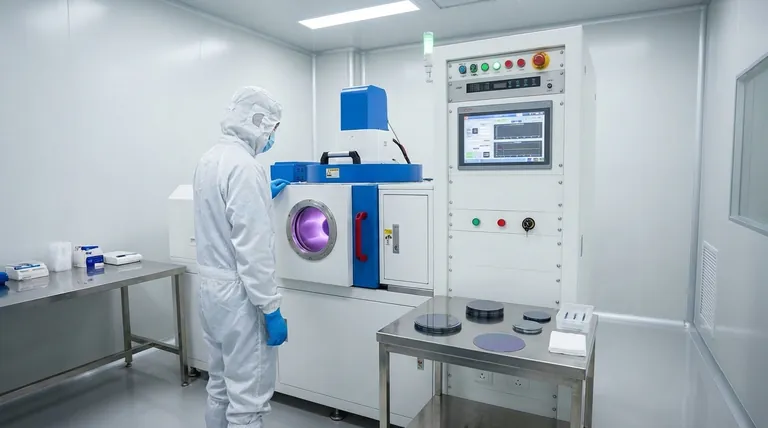
The Environment: The Sputter Coater System
Before the process can begin, the system's environment must be precisely controlled. This environment is created by a few critical components.
The Vacuum Chamber
The entire process takes place within a sealed chamber. A high-power vacuum pump removes air and contaminants like moisture to create an ultra-low-pressure environment, often around 10⁻⁶ torr. This pristine vacuum is essential to ensure the purity of the final film.
The Target Material
This is the source material you wish to deposit, such as gold, platinum, or a specific alloy. It is configured as a cathode, meaning it will be given a strong negative electrical charge.
The Substrate
This is the object you intend to coat, such as a silicon wafer, glass slide, or an electron microscopy sample. It is placed in the chamber to face the target.
The Inert Gas
An inert gas, most commonly Argon (Ar), is introduced into the chamber after the initial vacuum is established. This gas will not react chemically with the target or substrate; its sole purpose is to be ionized to create the sputtering effect.
The Sputtering Process, Step-by-Step
Once the system is prepared, the deposition process unfolds in a rapid, controlled sequence.
Step 1: Gas Ionization and Plasma Formation
A high voltage is applied across the chamber. This powerful electric field strips electrons from the Argon gas atoms, creating a mixture of free electrons and positively charged Argon ions (Ar+). This energized, glowing gas is known as a plasma.
Step 2: Ion Acceleration
Because the target material is set as the negative cathode, it strongly attracts the newly formed, positively charged Argon ions. The electric field accelerates these ions, causing them to rush toward the target at very high speeds.
Step 3: The Sputtering Event
The high-energy Argon ions collide with the surface of the target. This impact transfers a significant amount of kinetic energy, physically knocking atoms loose from the target material. These ejected atoms maintain a high level of energy.
Step 4: Deposition
The sputtered target atoms travel in a straight line through the low-pressure chamber until they strike the substrate. Upon impact, they condense on the surface, gradually building up a thin, uniform, and dense film.
Understanding the Trade-offs
Sputtering is a powerful and versatile technique, but it's essential to understand its advantages and limitations compared to other deposition methods.
Key Advantages of Sputtering
The primary strength of sputtering is its ability to deposit a vast range of materials. Because it's a physical and not a thermal process, it works exceptionally well for materials with high melting points and for complex alloys, which can be deposited while preserving their original chemical composition. The high energy of the sputtered atoms also typically results in films with excellent adhesion to the substrate.
Common Limitations
The deposition rate of sputtering is often slower than other methods like thermal evaporation. Furthermore, since the sputtered atoms travel in a straight line from the target, it is a "line-of-sight" process. This can make it challenging to uniformly coat substrates with complex, three-dimensional geometries without sophisticated substrate manipulation.
Making the Right Choice for Your Goal
Understanding the core principles of sputtering allows you to determine if it is the correct technique for your specific application.
- If your primary focus is coating a complex alloy: Sputtering is ideal because it maintains the material's stoichiometry from the target to the substrate.
- If your primary focus is depositing a refractory metal (e.g., tungsten, tantalum): Sputtering excels because it bypasses the need for the extreme temperatures required for evaporation.
- If your primary focus is achieving superior film adhesion and density: The high kinetic energy of the sputtered atoms creates a dense, well-adhered film that is difficult to achieve with other methods.
By mastering these fundamental steps and variables, you can precisely engineer high-quality thin films for a vast range of advanced applications.
Summary Table:
| Process Step | Key Component | Purpose |
|---|---|---|
| 1. Vacuum Creation | Vacuum Chamber & Pump | Removes air/contaminants for a pure deposition environment. |
| 2. Plasma Formation | Inert Gas (Argon) & High Voltage | Creates a plasma of ions (Ar+) to bombard the target. |
| 3. Sputtering Event | Target Material (Cathode) | High-energy ions knock atoms off the target surface. |
| 4. Film Deposition | Substrate | Sputtered atoms travel and condense, forming a thin, uniform film. |
Ready to Engineer Superior Thin Films with Precision?
Sputter coating is essential for achieving high-purity, uniform coatings for applications like electron microscopy, semiconductor manufacturing, and advanced materials research. The right equipment is critical to your success.
KINTEK specializes in high-performance lab equipment and consumables, serving the precise needs of laboratories like yours. We provide reliable sputter coaters and expert support to help you deposit everything from complex alloys to refractory metals with exceptional adhesion and density.
Let's discuss your specific coating challenges and goals. Contact our experts today to find the perfect sputter coating solution for your lab.
Visual Guide

Related Products
- Custom CVD Diamond Coating for Lab Applications
- HFCVD Machine System Equipment for Drawing Die Nano-Diamond Coating
- Chemical Vapor Deposition CVD Equipment System Chamber Slide PECVD Tube Furnace with Liquid Gasifier PECVD Machine
- Multifunctional Electrolytic Electrochemical Cell Water Bath Single Layer Double Layer
- Professional Cutting Tools for Carbon Paper Cloth Diaphragm Copper Aluminum Foil and More
People Also Ask
- What are the advantages of CVD coating? Superior Hardness and Uniformity for Demanding Applications
- What is CVD diamond coating? Grow a Super-Hard, High-Performance Diamond Layer
- What is CVD coating used for? Hardening Tools & Building Semiconductors for Industry
- How thick is CVD diamond coating? Balancing Durability and Stress for Optimal Performance
- What is CVD coating? Transform Your Material's Surface for Maximum Performance


