At its core, sputter coating is a vacuum deposition process that transfers material from a source (the "target") onto a surface (the "substrate") on an atom-by-atom basis. It works by bombarding the target with energized ions, which physically knock atoms loose. These ejected atoms then travel through a vacuum and condense on the substrate, forming an exceptionally thin and uniform film.
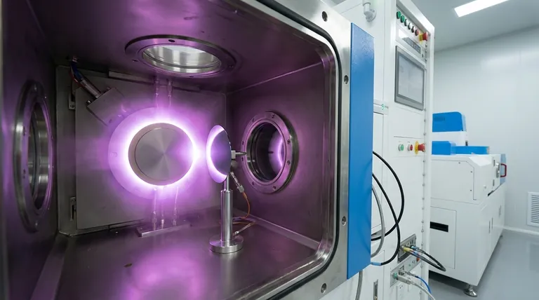
Sputter coating is fundamentally a process of atomic-level sandblasting in a vacuum. Instead of sand, it uses a plasma of ionized gas to bombard a material target, ejecting atoms that then coat a nearby object with a high-purity thin film.
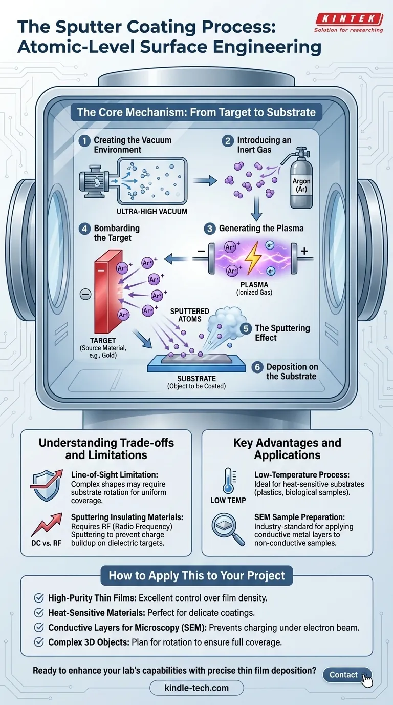
The Core Mechanism: From Target to Substrate
Understanding the sputtering process is to understand a highly controlled chain of events occurring within a vacuum chamber. Each step is critical for the final quality of the coating.
Step 1: Creating the Vacuum Environment
The entire process takes place in a sealed chamber where the air is pumped out to create a vacuum.
This vacuum is essential because it ensures the sputtered atoms can travel from the target to the substrate with minimal interference or contamination from air molecules like oxygen or nitrogen.
Step 2: Introducing an Inert Gas
Once a vacuum is achieved, a small, controlled amount of an inert gas, most commonly Argon (Ar), is introduced into the chamber.
This gas provides the raw material for the ions that will be used to bombard the target.
Step 3: Generating the Plasma
A high voltage is applied within the chamber, creating a powerful electric field. This field strips electrons from the Argon atoms, creating a mixture of positively charged Argon ions (Ar+) and free electrons.
This energized, ionized gas is known as a plasma, which often appears as a characteristic glow (typically purple for Argon).
Step 4: Bombarding the Target
The target, which is a block of the material you wish to deposit (e.g., gold, titanium, ceramic), is given a strong negative electrical charge.
The positively charged Argon ions in the plasma are aggressively accelerated toward the negatively charged target, striking its surface with significant kinetic energy.
Step 5: The Sputtering Effect
The impact of these high-energy ions is powerful enough to physically knock atoms loose from the target material. This ejection of atoms is the "sputtering" or "ablation" effect.
These sputtered atoms are ejected with very low thermal energy, essentially as a cool vapor.
Step 6: Deposition on the Substrate
The ejected atoms travel in a straight line from the target and land on the substrate—the object being coated.
Because the atoms arrive one by one, they build up an extremely thin, dense, and uniform film across the substrate's surface.
Understanding the Trade-offs and Limitations
While powerful, sputtering is not without its specific characteristics and challenges. Acknowledging them is key to using the technology effectively.
The Line-of-Sight Limitation
Sputtered atoms travel in a straight path from the target to the substrate. This is a "line-of-sight" process.
This means that coating complex, three-dimensional shapes with deep recesses or undercuts can be difficult. Achieving full coverage often requires rotating or manipulating the substrate during deposition.
Sputtering Insulating Materials
The standard process described above, known as DC sputtering, works well for electrically conductive targets. However, applying a constant negative voltage to an insulating (dielectric) target causes a buildup of positive charge that eventually repels the Argon ions and stops the process.
This is solved using RF (Radio Frequency) sputtering, which rapidly alternates the voltage. This alternating cycle prevents charge buildup and allows for the effective sputtering of ceramics and other insulators.
A Low-Temperature Advantage
A major advantage of sputtering is that it is a low-temperature process. The sputtered atoms themselves have very little heat.
This makes it ideal for coating heat-sensitive substrates such as plastics, polymers, and biological samples that would be damaged by higher-temperature coating methods. This is why it is used extensively in preparing samples for Scanning Electron Microscopy (SEM).
How to Apply This to Your Project
Your choice to use sputter coating should be driven by the specific requirements of your application, particularly the material properties you need to achieve.
- If your primary focus is creating a high-purity, uniform thin film: Sputtering is an excellent choice, as the vacuum environment and atomic deposition provide exceptional control over film density and purity.
- If your primary focus is coating heat-sensitive materials: Sputtering's low-temperature nature makes it one of the best methods for depositing films on plastics, polymers, or biological specimens.
- If your primary focus is a conductive layer for microscopy (SEM): Sputtering is the industry-standard method for applying a thin layer of conductive metal (like gold) to non-conductive samples to prevent charging under the electron beam.
- If your primary focus is coating complex 3D objects: You must account for the line-of-sight limitation and ensure your equipment allows for substrate rotation to achieve uniform coverage.
Ultimately, sputter coating offers a precise and versatile method for engineering surfaces at the atomic level, enabling the creation of advanced materials with tailored properties.
Summary Table:
| Step | Key Action | Purpose |
|---|---|---|
| 1 | Create Vacuum | Remove air to prevent contamination and allow atom travel |
| 2 | Introduce Inert Gas (Argon) | Provide ions for bombardment |
| 3 | Generate Plasma | Create energized ions and free electrons |
| 4 | Bombard Target | Accelerate ions to knock atoms loose from target material |
| 5 | Sputter Atoms | Eject target atoms as a cool vapor |
| 6 | Deposit on Substrate | Form thin, uniform film on the object being coated |
Ready to enhance your lab's capabilities with precise thin film deposition?
At KINTEK, we specialize in high-quality sputter coating systems and consumables designed for laboratory applications. Whether you're preparing samples for SEM, working with heat-sensitive materials, or developing advanced coatings, our expertise and equipment ensure superior results.
Contact us today to discuss your specific needs and discover how KINTEK can support your research and development goals with reliable, efficient lab solutions.
Visual Guide
Related Products
- Electron Beam Evaporation Coating Oxygen-Free Copper Crucible and Evaporation Boat
- Infrared Transmission Coating Sapphire Sheet Substrate Window
- Custom CVD Diamond Coating for Lab Applications
- 400-700nm Wavelength Anti Reflective AR Coating Glass
- Aluminized Ceramic Evaporation Boat for Thin Film Deposition
People Also Ask
- What is e-beam evaporation? Achieve High-Purity Thin Film Deposition for Your Lab
- What is e-beam evaporation used for? Precision Coating for Optics, Aerospace & Electronics
- What are the applications of e-beam evaporation? Achieve High-Purity Coatings for Optics & Electronics
- What is the container that holds the metal source material called in e-beam evaporation? Ensure Purity and Quality in Your Thin-Film Deposition
- What is the deposition rate of e-beam evaporation? Control Thin Film Quality and Speed


