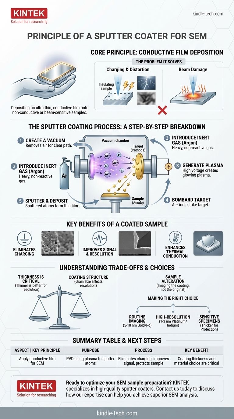
At its core, the principle of a sputter coater for SEM is to deposit an ultra-thin, electrically conductive film onto a non-conductive or beam-sensitive sample. This is achieved by creating a plasma in a vacuum, which uses high-energy ions to physically knock atoms off a metal target (like gold). These dislodged atoms then land on and coat the sample, rendering it suitable for high-quality imaging in a Scanning Electron Microscope.
The fundamental challenge in SEM is that the imaging electron beam requires a conductive path to ground. A sputter coater solves this by applying a micro-thin metallic "armor" to the sample, preventing electrical charging and beam damage that would otherwise destroy the image.

Why Sputter Coating is Essential for SEM
Before understanding how a coater works, it is critical to understand the problems it solves. An unprepared sample often produces poor, distorted, or non-existent images.
The Problem of "Charging"
Most biological specimens, polymers, ceramics, and glasses are electrical insulators.
When the SEM's high-energy electron beam strikes the surface of an insulating sample, the electrons accumulate. This buildup of negative charge, known as charging, deflects the incoming beam and severely distorts the resulting image, often creating bright patches, streaks, or drift.
The Risk of Beam Damage
The electron beam is a highly concentrated stream of energy. On delicate samples, this energy can cause localized heating, melting, or structural degradation.
This beam damage fundamentally alters the surface you are trying to observe, compromising the integrity of your analysis. The sputter coating acts as a protective shield.
The Sputter Coating Process: A Step-by-Step Breakdown
The sputtering process is a physical vapor deposition (PVD) technique that occurs within a small vacuum chamber. It is a precise and highly controlled method.
Step 1: Creating a Vacuum
The sample and a piece of target material (e.g., gold, platinum, or palladium) are placed inside a sealed chamber. A pump then removes the air, creating a low-pressure vacuum environment.
This vacuum is essential to ensure the sputtered atoms can travel to the sample without colliding with air molecules, which would disrupt the process.
Step 2: Introducing Inert Gas
A small, controlled amount of an inert gas, almost always Argon (Ar), is introduced into the chamber.
Argon is used because it is heavy and chemically non-reactive. It will not react with the sample or the target, ensuring a pure metal coating.
Step 3: Generating the Plasma
A high voltage is applied within the chamber, with the target material acting as the cathode (negative charge). This strong electric field strips electrons from the Argon atoms.
This process of ionization creates a plasma, a distinctive glowing cloud of positively charged Argon ions (Ar+) and free electrons.
Step 4: Bombarding the Target
The positively charged Argon ions are forcefully accelerated by the electric field and crash into the negatively charged target material.
This is a physical process of momentum transfer, where the heavy Argon ions act like sub-microscopic cannonballs.
Step 5: Sputtering and Deposition
The high-energy impact of the Argon ions is sufficient to knock atoms loose from the target material. This ejection of atoms is the "sputtering" effect.
These sputtered target atoms travel in straight lines through the vacuum chamber and deposit onto any surface they encounter, including your SEM sample. Over a period of seconds to minutes, these atoms build up to form a continuous, uniform thin film.
Key Benefits of a Coated Sample
A properly coated sample overcomes the primary obstacles to good SEM imaging, delivering several critical improvements simultaneously.
Eliminating Charging Artifacts
This is the primary benefit. The conductive metal layer provides a path for incoming electrons to travel to the grounded SEM stage, preventing charge buildup and the associated image distortions.
Improving Signal and Resolution
Metal coatings are excellent emitters of secondary electrons, which are the primary signal used to form an SEM image. A coated sample produces a stronger, clearer signal, leading to a better signal-to-noise ratio and sharper images with improved edge definition.
Enhancing Thermal Conduction
The metal film also helps to rapidly dissipate heat generated by the electron beam across the sample surface, protecting delicate structures from thermal damage.
Understanding the Trade-offs
While sputter coating is a powerful technique, it is not without considerations. An expert operator understands these trade-offs to optimize results.
Coating Thickness is Critical
The goal is to apply the thinnest possible coating that still provides the necessary conductivity. A coating that is too thick will obscure the fine nanoscale features of the sample's true surface.
The Coating Has Its Own Structure
The sputtered metal film is not perfectly smooth; it is composed of fine grains. For extremely high-magnification work, the grain size of the coating itself can become a limiting factor for resolution. The choice of target material (e.g., Gold/Palladium or Platinum) can influence this grain structure.
It Is an Alteration of the Sample
It is crucial to always remember that you are imaging the surface of the coating, not the original sample directly. While the coating conforms to the sample's topography, it is an added layer.
Making the Right Choice for Your Goal
Your coating strategy should be directly informed by your analytical objective.
- If your primary focus is routine imaging to eliminate charging: A standard gold or gold/palladium coating of 5-10 nm is an excellent and cost-effective choice.
- If your primary focus is high-resolution imaging (FEG-SEM): You must use the thinnest possible coating (1-3 nm) of a fine-grained material like platinum or iridium to preserve the finest surface details.
- If your primary focus is protecting highly sensitive specimens: A slightly thicker coating can provide superior thermal and physical protection from the beam, even if it sacrifices some ultimate resolution.
Mastering the principles of sputter coating is fundamental to unlocking the full analytical power of your scanning electron microscope.
Summary Table:
| Aspect | Key Principle |
|---|---|
| Purpose | Apply a conductive film to non-conductive samples for SEM imaging. |
| Process | Physical Vapor Deposition (PVD) using plasma to sputter target atoms. |
| Key Benefit | Eliminates charging artifacts, improves signal, and protects the sample. |
| Key Consideration | Coating thickness and material choice are critical for resolution and sample integrity. |
Ready to optimize your SEM sample preparation?
KINTEK specializes in providing high-quality sputter coaters and lab equipment tailored to your laboratory's needs. Our solutions ensure precise, uniform coatings to eliminate charging and enhance your imaging results.
Contact us today to discuss how our expertise can help you achieve superior SEM analysis. Get in touch via our contact form and let's improve your lab's capabilities together.
Visual Guide
Related Products
- Professional Cutting Tools for Carbon Paper Cloth Diaphragm Copper Aluminum Foil and More
- Custom CVD Diamond Coating for Lab Applications
- Multifunctional Electrolytic Electrochemical Cell Water Bath Single Layer Double Layer
- HFCVD Machine System Equipment for Drawing Die Nano-Diamond Coating
- Reference Electrode Calomel Silver Chloride Mercury Sulfate for Laboratory Use
People Also Ask
- What are carbon cloths used for? Conquer Static Dust on Electronics & Screens
- How is carbon paper treated for use in fuel cells? The Critical PTFE Coating for Peak Performance
- What are the typical uses for carbon paper? Powering Fuel Cells and Advanced Research
- How should carbon paper be handled during cutting? Prevent Fractures with a Delicate, Precise Approach
- Why is carbon paper placed between the powder and the graphite mold? Protect Your LTPO Electrolytes & Tooling


