In essence, sputtering is a physical vapor deposition (PVD) technique used to deposit a thin film of material onto a surface, known as a substrate. The process can be visualized as an atomic-scale billiards game: high-energy ions are shot at a source material, called the target, knocking atoms off its surface. These dislodged atoms then travel through a vacuum and coat the substrate, forming a new, ultra-thin layer that is fundamental to creating modern microchips.
Sputtering is not a chemical reaction but a purely physical process of momentum transfer. Its value lies in the exceptional control it provides over the thickness, purity, and structural properties of the deposited films, making it an indispensable tool in semiconductor manufacturing.
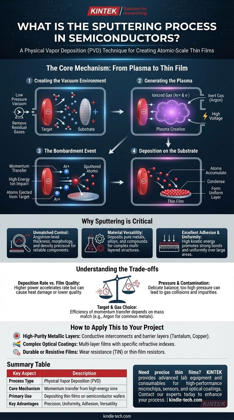
The Core Mechanism: From Plasma to Thin Film
Sputtering is a multi-stage process that takes place inside a controlled vacuum chamber. Each step is critical to achieving a high-quality, uniform thin film.
Step 1: Creating the Vacuum Environment
The entire process begins by placing the target (the source material) and the substrate (the component to be coated, like a silicon wafer) into a chamber. This chamber is then pumped down to a very low pressure, creating a vacuum.
This initial step is crucial for removing residual gases like oxygen and water vapor, which could otherwise contaminate the film and compromise its electrical or physical properties.
Step 2: Generating the Plasma
Once a clean vacuum is established, a small, precisely controlled amount of an inert gas—almost always Argon (Ar)—is introduced into the chamber.
A high voltage is then applied. This electrical energy strips electrons from the Argon atoms, creating a mixture of positively charged Argon ions (Ar+) and free electrons. This energized, ionized gas is known as a plasma.
Step 3: The Bombardment Event
The target material is given a strong negative electrical charge. This causes the positively charged Argon ions from the plasma to accelerate aggressively toward the target.
These high-velocity ions collide with the target surface, transferring their kinetic energy and momentum. This impact is powerful enough to physically knock out, or "sputter," individual atoms from the target material.
Step 4: Deposition on the Substrate
The ejected atoms from the target travel through the low-pressure chamber and land on the surface of the substrate.
Over time, these atoms accumulate and condense, nucleating and growing into a continuous, uniform thin film. The final properties of this film—such as its density, grain structure, and electrical resistivity—can be precisely controlled.
Why Sputtering is Critical in Semiconductor Fabrication
Sputtering isn't just one of many options; it is a foundational technology for manufacturing integrated circuits, displays, and sensors due to its unique advantages.
Unmatched Control Over Film Properties
Sputtering allows for Angstrom-level precision over film thickness. By carefully managing process parameters like pressure, power, and time, engineers can dictate the film's morphology, grain size, and density. This control is essential for creating reliable electronic components.
Versatility in Materials
The physical nature of sputtering allows it to deposit a vast range of materials. This includes pure metals (like Tantalum and Copper for wiring), alloys, and even insulating or semiconducting compounds. This flexibility is vital for building the complex, multi-layered structures of a modern microchip.
Excellent Adhesion and Uniformity
Sputtered atoms arrive at the substrate with significant kinetic energy, which promotes strong adhesion to the surface. Furthermore, by rotating the substrate or using carefully designed magnetrons to shape the plasma, sputtering can achieve excellent film uniformity over large areas, such as a 300mm silicon wafer.
Understanding the Trade-offs
While powerful, sputtering is a process of balancing competing factors. Understanding these trade-offs is key to its successful implementation.
Deposition Rate vs. Film Quality
Increasing the power applied to the target will accelerate more ions, increasing the deposition rate. However, excessive power can generate too much heat, potentially damaging the substrate or creating a less-ordered, lower-quality film.
Pressure and Contamination
The chamber pressure presents a delicate balance. It must be high enough to sustain a stable plasma and provide enough Argon ions for an efficient sputtering rate. If the pressure is too high, sputtered atoms may collide with gas atoms on their way to the substrate, reducing uniformity and potentially incorporating impurities.
Target Material and Gas Choice
The efficiency of the momentum transfer depends on the relative masses of the sputtering gas ion and the target atom. Maximum energy transfer occurs when the masses are equal. This is why Argon is an excellent, cost-effective choice for sputtering many common mid-weight metals.
How to Apply This to Your Project
The decision to use sputtering is determined by the specific film properties your application demands.
- If your primary focus is high-purity metallic layers: Sputtering is the industry standard for creating the conductive interconnects and barrier layers (e.g., Tantalum, Copper, Aluminum) inside a chip.
- If your primary focus is complex optical coatings: The precise thickness control offered by sputtering makes it ideal for depositing multi-layer films with specific refractive indexes for lenses, filters, and displays.
- If your primary focus is durable or resistive films: Sputtering can deposit hard, dense coatings like titanium nitride (TiN) for wear resistance or resistive materials for thin-film resistors.
By mastering this atomic-scale construction process, we enable the creation of virtually all modern electronic devices.
Summary Table:
| Key Aspect | Description |
|---|---|
| Process Type | Physical Vapor Deposition (PVD) |
| Core Mechanism | Momentum transfer from high-energy ions (e.g., Argon) to a target material |
| Primary Use | Depositing thin films (metals, alloys, compounds) onto semiconductor wafers |
| Key Advantages | Angstrom-level thickness control, excellent film uniformity, strong adhesion, material versatility |
Need precise thin films for your semiconductor or lab project? The sputtering process is fundamental for creating high-performance microchips, sensors, and optical coatings. At KINTEK, we specialize in providing the advanced lab equipment and consumables needed to achieve these results. Our expertise ensures you get the control over film purity, thickness, and structure that your research or production demands.
Contact our experts today to discuss how our solutions can enhance your thin film deposition process.
Visual Guide
Related Products
- Spark Plasma Sintering Furnace SPS Furnace
- Vacuum Induction Melting Spinning System Arc Melting Furnace
- Chemical Vapor Deposition CVD Equipment System Chamber Slide PECVD Tube Furnace with Liquid Gasifier PECVD Machine
- Customer Made Versatile CVD Tube Furnace Chemical Vapor Deposition Chamber System Equipment
People Also Ask
- What is the process fundamentals of spark plasma sintering? Achieve Rapid, High-Density Material Consolidation
- What is the difference between spark plasma sintering and flash sintering? A Guide to Advanced Sintering Methods
- What is the mechanism of SPS process? A Deep Dive into Rapid, Low-Temperature Sintering
- What are the advantages of CAMI/SPS for W-Cu composite preparation? Reduce cycles from hours to seconds.
- What are the fundamentals of spark plasma sintering process? Unlock Rapid, High-Performance Material Consolidation


