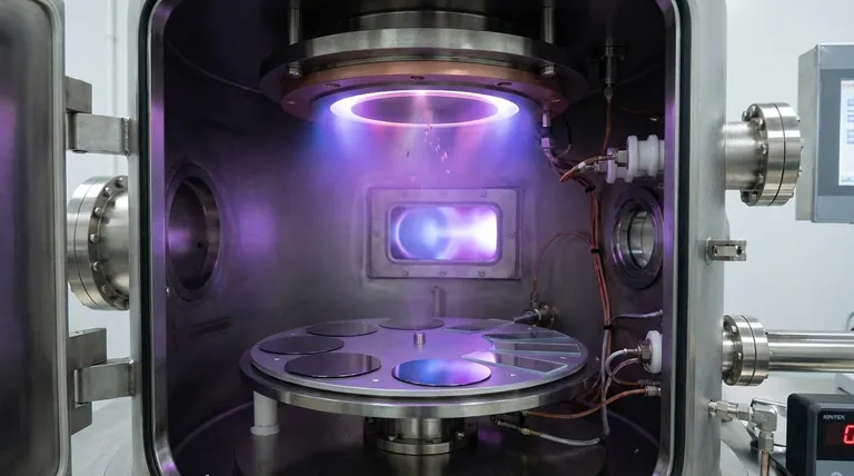
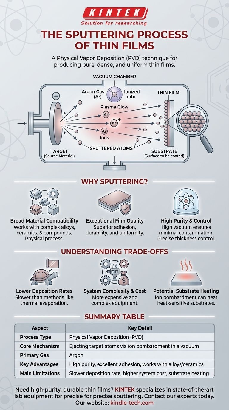
In the simplest terms, sputtering is a physical process used to deposit an exceptionally thin layer of material onto a surface. It works by ejecting atoms from a source material (called a "target") by bombarding it with energized ions inside a vacuum chamber. These ejected atoms then travel and coat a secondary surface (the "substrate"), forming the thin film.
Sputtering is a highly controlled and versatile Physical Vapor Deposition (PVD) technique. Its core value lies in its ability to produce very pure, dense, and uniform thin films from a vast range of materials, making it a cornerstone of modern manufacturing.
The Core Mechanism: From Ion to Film
To understand sputtering, it helps to visualize it as a microscopic game of atomic billiards. The entire process takes place inside a sealed vacuum chamber to prevent contamination.
Step 1: Creating the Environment
The process begins by creating a high vacuum in a chamber. A small amount of an inert gas, typically Argon, is then introduced. This gas provides the "projectiles" needed for the next step.
Step 2: Energizing the Ions
A powerful electric field is applied within the chamber, which strips electrons from the Argon atoms, turning them into positively charged ions. This creates a plasma, often visible as a characteristic glow.
Step 3: Bombarding the Target
The source material to be deposited, known as the target, is given a negative charge. This powerful negative potential aggressively attracts the positively charged Argon ions, causing them to accelerate and slam into the target with significant force.
Step 4: Deposition on the Substrate
This high-energy collision physically knocks atoms loose from the target material, "sputtering" them away. These ejected atoms travel in a straight line through the vacuum until they strike the object being coated—the substrate—where they condense and build up, layer by layer, to form a thin film.
Why Sputtering is a Foundational Technique
While several methods exist for creating thin films, sputtering is exceptionally common due to its unique advantages in control and material flexibility.
Broad Material Compatibility
Unlike some methods that rely on melting and evaporating materials, sputtering is a physical process. This means it can be used to deposit almost any material, including complex alloys, ceramics, and compounds, without altering their chemical composition.
Exceptional Film Quality
The kinetic energy of the sputtered atoms helps them form a very dense and tightly packed film on the substrate. This results in coatings with superior adhesion, durability, and uniformity compared to other techniques.
High Purity and Control
Because the process occurs in a high vacuum, there are very few stray molecules to contaminate the film. This allows for the creation of extremely pure coatings. Furthermore, the rate of deposition can be precisely controlled, allowing for films of a specific, repeatable thickness down to the atomic level.
Understanding the Trade-offs
No single process is perfect for every application. Building trust requires acknowledging the limitations of a technique.
Lower Deposition Rates
Sputtering is generally a slower process compared to other methods like thermal evaporation. When the goal is to deposit a very thick coating quickly, sputtering may not be the most efficient choice.
System Complexity and Cost
Sputtering systems, with their high-vacuum pumps, power supplies, and control electronics, are more complex and expensive than simpler deposition methods.
Potential Substrate Heating
The constant bombardment of atoms and ions can transfer a significant amount of energy to the substrate, causing it to heat up. This can be a challenge when coating heat-sensitive materials like certain plastics or organic compounds.
Making the Right Choice for Your Application
Selecting a deposition method depends entirely on the desired outcome for the final product.
- If your primary focus is high-purity, dense coatings with strong adhesion: Sputtering is almost always the superior choice, especially for complex materials like alloys or optical coatings.
- If your primary focus is depositing a simple metal film as quickly and cheaply as possible: A technique like thermal evaporation might be a more practical alternative.
- If your primary focus is coating a complex, three-dimensional shape with a uniform layer: A non-line-of-sight method like Chemical Vapor Deposition (CVD) may be better suited for the task.
Ultimately, understanding the core principles of sputtering empowers you to select the right tool for creating high-performance materials.
Summary Table:
| Aspect | Key Detail |
|---|---|
| Process Type | Physical Vapor Deposition (PVD) |
| Core Mechanism | Ejecting target atoms via ion bombardment in a vacuum |
| Primary Gas Used | Argon |
| Key Advantages | High purity, excellent adhesion, works with alloys/ceramics |
| Main Limitations | Slower deposition rate, higher system cost, substrate heating |
Need a high-purity, durable thin film for your project? Sputtering is the ideal solution for demanding applications in semiconductor manufacturing, advanced optics, and R&D. KINTEK specializes in providing state-of-the-art lab equipment and consumables for precise sputtering processes. Our expertise ensures you achieve the uniform, contaminant-free coatings your work requires. Contact our experts today to discuss how we can support your laboratory's thin film deposition needs.
Visual Guide
Related Products
- Spark Plasma Sintering Furnace SPS Furnace
- Vacuum Induction Melting Spinning System Arc Melting Furnace
- Chemical Vapor Deposition CVD Equipment System Chamber Slide PECVD Tube Furnace with Liquid Gasifier PECVD Machine
- Customer Made Versatile CVD Tube Furnace Chemical Vapor Deposition Chamber System Equipment
People Also Ask
- Why are Spark Plasma Sintering (SPS) furnaces or hot presses utilized in the preparation of Li3PS4 solid electrolytes?
- What is the difference between spark plasma sintering and flash sintering? A Guide to Advanced Sintering Methods
- What is the pressure for spark plasma sintering? A Guide to Optimizing SPS Parameters
- What technical advantages does a Spark Plasma Sintering (SPS) furnace offer for LZP ceramics? Enhance Ionic Conductivity
- What are the fundamentals of spark plasma sintering process? Unlock Rapid, High-Performance Material Consolidation


