Sputter coating is a foundational technology used to apply ultra-thin, high-performance films of material onto a surface. It is a critical process in advanced manufacturing, enabling the creation of components for industries ranging from microelectronics and solar panels to architectural glass and aerospace.
The core purpose of sputter coating is not just to apply a layer, but to do so with exceptional uniformity and durability. It achieves this by using a physical process—ion bombardment in a vacuum—to create a dense, consistent film that is difficult to replicate with other methods.
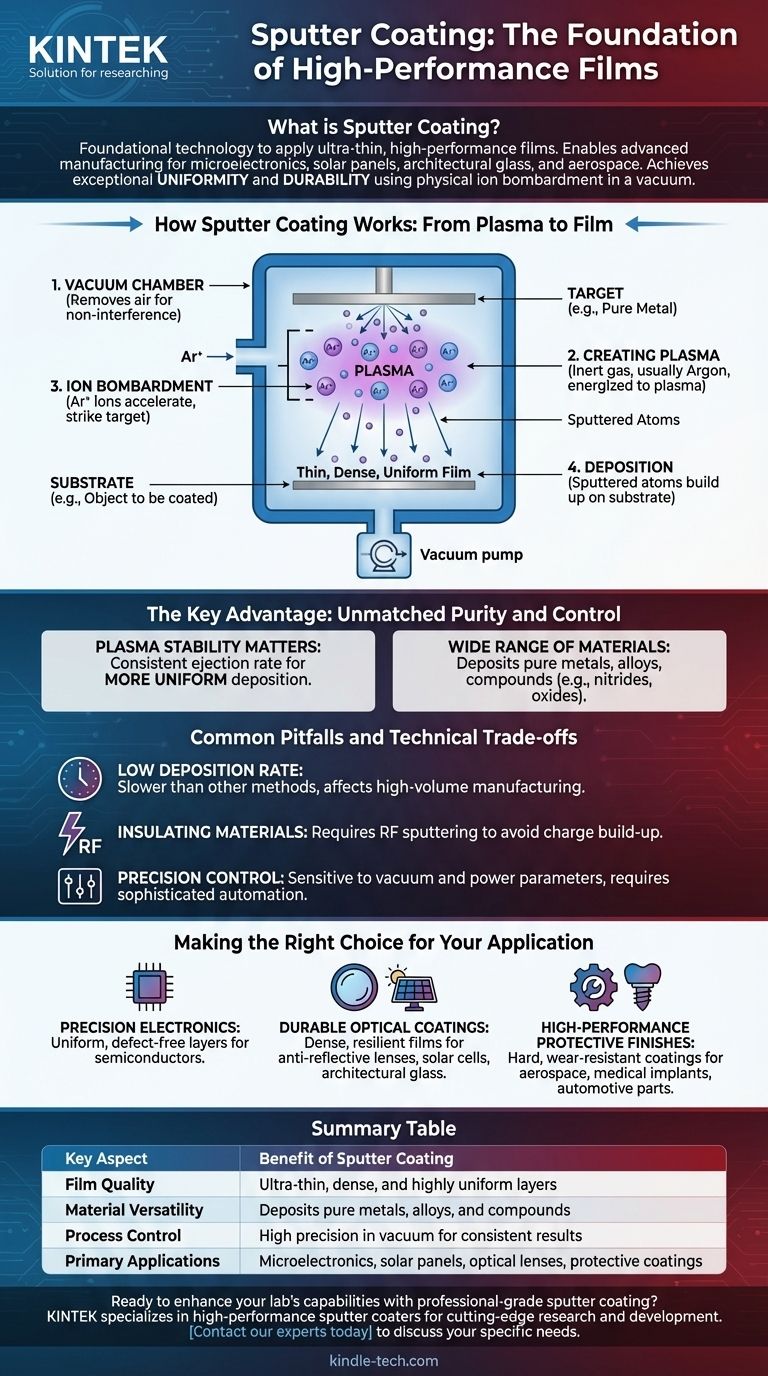
How Sputter Coating Works: From Plasma to Film
Sputter coating is a physical vapor deposition (PVD) method. The process physically displaces atoms from a source material and deposits them onto the desired object, all within a highly controlled environment.
The Role of the Vacuum Chamber
The entire process takes place inside a vacuum chamber. This is critical because it removes air and other particles, ensuring the ejected material atoms can travel to the target surface without interference or contamination.
Creating the Plasma
A small amount of an inert gas, typically argon, is introduced into the chamber. An electric field is applied, which energizes the gas and turns it into a plasma, an ionized state of matter often seen as a glow discharge.
Ion Bombardment of the Target
This plasma contains positively charged argon ions. These ions are accelerated by the electric field and directed with great force toward the source material, known as the target.
When these high-energy ions strike the target, they physically knock out, or "sputter," microscopic particles and atoms from the target's surface.
Deposition on the Substrate
These sputtered atoms travel through the vacuum and land on the object being coated, which is called the substrate. They gradually build up on the substrate, forming a very thin, dense, and highly uniform film.
The Key Advantage: Unmatched Purity and Control
The reason sputter coating is so widely adopted is its ability to produce superior quality films. This stems directly from the physics of the process.
Why Plasma Stability Matters
The stable and controlled nature of the plasma ensures that atoms are ejected from the target at a consistent rate and energy. This directly translates to a more uniform and even deposition across the entire substrate surface.
A Wide Range of Materials
The sputtering process is remarkably versatile. It can be used to deposit films of pure metals, alloys, and compounds like titanium, chromium, zirconium nitrides, and various oxides.
Common Pitfalls and Technical Trade-offs
While powerful, sputter coating is not without its challenges. Understanding its limitations is key to using it effectively.
The Challenge of Deposition Speed
Traditional DC sputtering methods can have a relatively low deposition rate. This means the process can be slower compared to other coating techniques, which is a factor in high-volume manufacturing.
Difficulty with Insulating Materials
Simple DC diode sputtering works well for conductive materials. However, it cannot effectively sputter insulating materials because a charge builds up on the target surface, repelling the ions. More complex techniques like RF sputtering are required for insulators.
The Need for Precision Control
The process is highly sensitive to parameters like vacuum pressure and power levels. Achieving consistent results often requires sophisticated automation, as manual control can be less reliable.
Making the Right Choice for Your Application
Selecting a coating process depends entirely on your end goal. Sputtering excels where film quality and performance are non-negotiable.
- If your primary focus is precision electronics: Sputter coating provides the uniform, defect-free conductive and insulating layers essential for fabricating modern semiconductors.
- If your primary focus is durable optical coatings: The process creates the dense, resilient films needed for anti-reflective lenses, solar cells, and low-emissivity architectural glass.
- If your primary focus is high-performance protective finishes: Sputtering applies hard, wear-resistant coatings to aerospace components, medical implants, and automotive parts with exceptional consistency.
Ultimately, sputter coating is the definitive choice when the performance and reliability of a surface film are as critical as the product itself.
Summary Table:
| Key Aspect | Benefit of Sputter Coating |
|---|---|
| Film Quality | Ultra-thin, dense, and highly uniform layers |
| Material Versatility | Deposits pure metals, alloys, and compounds (e.g., nitrides, oxides) |
| Process Control | High precision in a vacuum environment for consistent results |
| Primary Applications | Microelectronics, solar panels, optical lenses, protective coatings |
Ready to enhance your lab's capabilities with professional-grade sputter coating?
KINTEK specializes in high-performance lab equipment, including sputter coaters, to help you achieve the precise, durable thin films required for cutting-edge research and development in microelectronics, optics, and material science. Our solutions are designed for reliability and superior results.
Contact our experts today to discuss how our sputter coating systems can meet your specific application needs.
Visual Guide
Related Products
- Infrared Transmission Coating Sapphire Sheet Substrate Window
- Electron Beam Evaporation Coating Oxygen-Free Copper Crucible and Evaporation Boat
- 400-700nm Wavelength Anti Reflective AR Coating Glass
- Custom CVD Diamond Coating for Lab Applications
- Molybdenum Tungsten Tantalum Special Shape Evaporation Boat
People Also Ask
- What is organic thin film? A Guide to Engineered Molecular Layers for Advanced Tech
- What is optical coating used for? Control Light for Enhanced Performance in Your Applications
- What is the optical coating? Master Light Control for Superior Optical Performance
- How can we create a reducing environment? Master the Methods for Precise Chemical Control
- Is Sputter Tint good? Premium Heat Rejection & Long-Term Durability Explained


