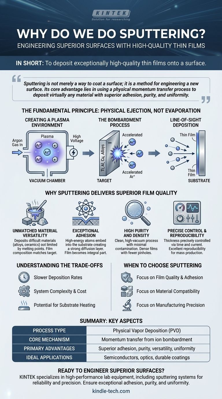
In short, we use sputtering to deposit exceptionally high-quality thin films onto a surface. It is a premier manufacturing process valued for creating coatings that are dense, pure, and adhere strongly to the substrate, making it indispensable for high-performance applications in industries like semiconductors and precision optics.
Sputtering is not merely a way to coat a surface; it is a method for engineering a new surface. Its core advantage lies in using a physical momentum transfer process, rather than heat, to deposit virtually any material with superior adhesion, purity, and uniformity.
The Fundamental Principle: Physical Ejection, Not Evaporation
To understand why sputtering is so effective, you must first grasp that it is a Physical Vapor Deposition (PVD) process. Unlike thermal evaporation, which boils a material, sputtering is more like an atomic-scale sandblasting operation.
Creating a Plasma Environment
The process begins in a vacuum chamber, which is pumped down to remove contaminants. A small amount of an inert process gas, typically Argon, is then introduced.
A high voltage is applied, which strips electrons from the argon atoms. This creates a plasma, which is a highly ionized gas containing positively charged argon ions and free electrons.
The Bombardment Process
A solid slab of the material to be deposited, known as the target, is given a strong negative electrical charge.
The positively charged argon ions in the plasma are aggressively accelerated toward this negatively charged target. They collide with the target with significant force.
Line-of-Sight Deposition
This high-energy bombardment physically knocks atoms or molecules out of the target material. These ejected particles travel in a straight line through the vacuum chamber.
When these particles strike a component placed in their path—the substrate—they stick to it, gradually building up a thin, uniform film.
Why Sputtering Delivers Superior Film Quality
The "why" of sputtering is found in the unique characteristics of the film it produces. The physical nature of the process gives it distinct advantages over other methods.
Unmatched Material Versatility
Because sputtering physically ejects atoms, it is not limited by a material's melting point. This allows for the deposition of a vast range of materials that are difficult or impossible to deposit using thermal evaporation.
This includes high-melting-point metals, complex alloys, ceramics, and other compounds. The composition of the sputtered film is an excellent match for the composition of the target.
Exceptional Adhesion
Sputtered atoms arrive at the substrate with significantly higher kinetic energy than evaporated atoms. This high energy allows them to embed slightly into the substrate surface.
This process forms a tight interfacial or diffusion layer, resulting in adhesion that is far stronger than what can be achieved with many other coating techniques. The film becomes an integral part of the substrate rather than just a layer sitting on top.
High Purity and Density
Sputtering is a clean process. Since it occurs in a high vacuum and doesn't involve heating a source material to extreme temperatures in a crucible, there are far fewer opportunities for contamination.
The result is a film that is highly pure and dense, with fewer pinholes or structural defects. This is critical for applications in optics and electronics where impurities can degrade performance.
Precise Control and Reproducibility
The film's thickness can be precisely controlled by managing the sputtering time and the electrical current applied to the target.
This allows for excellent reproducibility from one run to the next, which is essential for mass production. Sputtering can also produce highly uniform films over very large surface areas.
Understanding the Trade-offs
No process is perfect. To make an informed decision, you must be aware of sputtering's limitations.
Slower Deposition Rates
Generally, sputtering is a slower process compared to a technique like thermal evaporation. For applications where a thick coating is needed quickly and ultimate quality is not the primary driver, sputtering may not be the most efficient choice.
System Complexity and Cost
Sputtering systems are mechanically complex, requiring high-vacuum chambers, sophisticated power supplies, and often magnetic fields (in magnetron sputtering) to enhance efficiency. This makes the initial equipment investment higher than for simpler deposition methods.
Potential for Substrate Heating
The constant bombardment of high-energy particles can transfer heat to the substrate. While often minimal, this can be a concern when coating temperature-sensitive materials like certain plastics or biological samples.
When to Choose Sputtering
Your choice of deposition method should be driven by the specific requirements of your final product.
- If your primary focus is film quality and adhesion: Sputtering is the superior choice for mission-critical applications where coatings must be durable, dense, and strongly bonded.
- If your primary focus is material compatibility: Sputtering is essential when working with alloys, compounds, or high-melting-point materials that are difficult to evaporate.
- If your primary focus is manufacturing precision: Sputtering provides the control and reproducibility needed for high-volume production of sensitive devices like semiconductors and optical filters.
- If your primary focus is speed and low cost for simple metals: Thermal evaporation may be a more practical alternative for less demanding applications.
Ultimately, sputtering is the industry standard when the performance and reliability of the thin film are paramount.
Summary Table:
| Key Aspect | Why It Matters |
|---|---|
| Process Type | Physical Vapor Deposition (PVD) |
| Core Mechanism | Momentum transfer from ion bombardment (e.g., Argon) |
| Primary Advantages | Superior adhesion, high purity, material versatility, excellent uniformity |
| Ideal Applications | Semiconductors, precision optics, durable decorative coatings |
| Main Considerations | Slower deposition rates, higher system complexity and cost |
Ready to engineer superior surfaces with sputtering?
KINTEK specializes in high-performance lab equipment, including sputtering systems designed for reliability and precision. Whether you are developing next-generation semiconductors, advanced optical coatings, or durable thin films, our expertise ensures you achieve the exceptional adhesion, purity, and uniformity your application demands.
Contact our experts today to discuss how our sputtering solutions can enhance your manufacturing process and product performance.
Visual Guide
Related Products
- Chemical Vapor Deposition CVD Equipment System Chamber Slide PECVD Tube Furnace with Liquid Gasifier PECVD Machine
- Spark Plasma Sintering Furnace SPS Furnace
- Vacuum Induction Melting Spinning System Arc Melting Furnace
- Split Chamber CVD Tube Furnace with Vacuum Station Chemical Vapor Deposition System Equipment Machine
- Multi Heating Zones CVD Tube Furnace Machine Chemical Vapor Deposition Chamber System Equipment
People Also Ask
- What happens during deposition chemistry? Building Thin Films from Gaseous Precursors
- How are carbon nanotubes grown? Master Scalable Production with Chemical Vapor Deposition
- What is plasma enhanced chemical vapor deposition PECVD equipment? A Guide to Low-Temperature Thin Film Deposition
- What types of substrates are used in CVD to facilitate graphene films? Optimize Graphene Growth with the Right Catalyst
- What are the processes of vapor phase deposition? Understand CVD vs. PVD for Superior Thin Films


