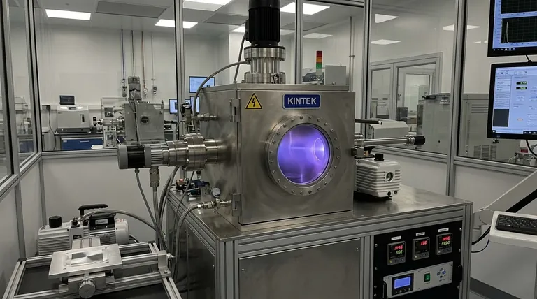
In essence, sputter coating is used to apply an exceptionally uniform, dense, and strongly bonded thin film of material onto a surface. This physical deposition process offers unparalleled control over the coating's thickness and composition, making it a critical technique in fields ranging from semiconductor manufacturing to high-resolution scientific imaging.
Sputter coating is chosen over other methods not just for its ability to apply a coating, but for the superior quality of that coating. The process physically bombards a target to create a stable plasma, resulting in a film with unmatched uniformity, density, and adhesion that other techniques struggle to replicate.
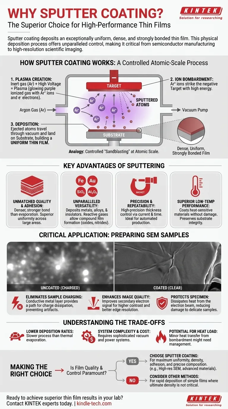
How Sputter Coating Works: A Controlled Collision
Sputter coating is a type of physical vapor deposition (PVD) that operates within a vacuum. The underlying principle is best understood as a highly controlled process of atomic-scale "sandblasting," where individual atoms are ejected from a source material and redeposited onto a sample.
Creating the Plasma
The process begins by introducing an inert gas, typically Argon, into a vacuum chamber. A high voltage is applied, which strips electrons from the Argon atoms, creating a plasma—a glowing, ionized gas containing positive Argon ions and free electrons.
The Target and Ion Bombardment
A block of the desired coating material, known as the target, is given a negative electrical charge. The positively charged Argon ions in the plasma are forcefully accelerated toward this negative target, striking its surface with significant energy.
Deposition onto the Substrate
This high-energy bombardment physically dislodges or "sputters" atoms from the target material. These ejected atoms travel through the vacuum chamber and land on the surface of the object being coated (the substrate), gradually building up a thin, uniform film.
Key Advantages of the Sputtering Process
The physical nature of sputter coating provides several distinct advantages over other methods like simple thermal evaporation.
Unmatched Film Quality and Adhesion
Because the sputtered atoms arrive at the substrate with higher energy than evaporated atoms, they form a denser and more strongly bonded film. The stable plasma ensures a highly uniform deposition across large areas, which is critical for consistent performance.
Unparalleled Material Versatility
Sputtering can be used to deposit a vast range of materials, including metals, alloys, and even insulators. By introducing reactive gases (like oxygen or nitrogen) into the chamber, it's possible to form compound films like oxides or nitrides from a pure metal target.
Precision and Repeatability
The thickness of the sputtered film is directly proportional to the target's input current and the coating time. This relationship allows for high-precision control over film thickness, making the process highly repeatable and suitable for automated, continuous production.
Superior Low-Temperature Performance
Compared to other techniques that require high heat, sputter coating can produce dense, crystalline films at much lower substrate temperatures. This makes it ideal for coating heat-sensitive materials that would otherwise be damaged.
A Critical Application: Preparing SEM Samples
One of the most common uses for sputter coating is preparing non-conductive samples for Scanning Electron Microscopy (SEM). An SEM uses an electron beam to create an image, which presents several challenges that sputtering solves directly.
Eliminating Sample Charging
Non-conductive samples (like biological specimens or ceramics) accumulate electrical charge from the electron beam, causing image distortion and artifacts. A thin, sputtered layer of a conductive metal, like gold or platinum, provides a path for this charge to dissipate.
Enhancing Image Quality and Resolution
The metallic coating dramatically improves the emission of secondary electrons from the sample's surface. These electrons are what the SEM detector uses to form an image, so a stronger signal results in a clearer, higher-contrast image with better edge resolution.
Protecting the Specimen
The sputter-coated layer also serves a protective function. It helps to conduct heat away from the sample, preventing damage from the focused electron beam, which is especially important for delicate, beam-sensitive specimens.
Understanding the Trade-offs
While powerful, sputter coating is not the ideal solution for every situation. Its primary trade-offs are related to speed and complexity.
Lower Deposition Rates
Generally, sputter coating is a slower process compared to a technique like thermal evaporation. The rate of material deposition is lower, which can increase processing time for very thick films.
System Complexity and Cost
Sputtering systems require a sophisticated vacuum chamber, high-voltage power supplies, and precise gas flow controllers. This makes the equipment more complex and expensive than simpler coating methods.
Potential for Heat Load
Although it is a low-temperature process overall, the constant bombardment of atoms can transfer some heat to the substrate. For extremely temperature-sensitive substrates, this minor heat load may need to be managed.
Making the Right Choice for Your Application
Selecting the right coating technology depends entirely on your end goal. Sputtering excels where film quality and control are non-negotiable.
- If your primary focus is maximum uniformity, density, and adhesion for a high-performance coating: Sputter coating is the superior technical choice.
- If your primary focus is preparing a non-conductive or delicate sample for high-resolution SEM imaging: Sputtering is the industry-standard method for achieving optimal results.
- If your primary focus is creating precise alloy or compound films: The control offered by sputtering is essential for maintaining the correct composition.
- If your primary focus is rapid deposition of a simple metal film where ultimate density is not critical: A less complex method like thermal evaporation might be a more cost-effective solution.
Ultimately, sputter coating is chosen when the precision, quality, and performance of the thin film are paramount to the success of the application.
Summary Table:
| Aspect | Key Advantage |
|---|---|
| Film Quality | Unmatched uniformity, density, and strong adhesion |
| Material Versatility | Deposits metals, alloys, and insulators |
| Process Control | High-precision thickness and composition control |
| Key Application | Essential for preparing non-conductive samples for SEM imaging |
Ready to achieve superior thin film results in your lab?
KINTEK specializes in high-performance sputter coating equipment and consumables, designed to meet the precise demands of semiconductor manufacturing, materials science research, and SEM sample preparation. Our solutions deliver the uniformity, adhesion, and control your applications require.
Contact our experts today to discuss how our sputter coating systems can enhance your laboratory's capabilities and drive your research forward.
Visual Guide
Related Products
- Custom CVD Diamond Coating for Lab Applications
- HFCVD Machine System Equipment for Drawing Die Nano-Diamond Coating
- Chemical Vapor Deposition CVD Equipment System Chamber Slide PECVD Tube Furnace with Liquid Gasifier PECVD Machine
- Multifunctional Electrolytic Electrochemical Cell Water Bath Single Layer Double Layer
- Professional Cutting Tools for Carbon Paper Cloth Diaphragm Copper Aluminum Foil and More
People Also Ask
- What are the different CVD coating? A Guide to Thermal CVD, PECVD, and Specialized Methods
- What are the advantages of CVD coating? Superior Hardness and Uniformity for Demanding Applications
- What is CVD diamond coating? Grow a Super-Hard, High-Performance Diamond Layer
- How thick is CVD diamond coating? Balancing Durability and Stress for Optimal Performance
- What is CVD coated? A Guide to Superior Wear Resistance for Complex Parts


