RF (Radio Frequency) power is used in sputtering primarily to deposit thin films from non-conductive, or insulating, target materials. Unlike Direct Current (DC) sputtering, which only works with conductive targets, the alternating nature of an RF field prevents the buildup of electrical charge on the insulator's surface, which would otherwise stop the process entirely.
The fundamental reason for using RF sputtering is to overcome a critical limitation of DC sputtering: the inability to work with insulating materials. The alternating RF field acts as a electrical reset switch, continuously neutralizing the positive charge that would otherwise build up on an insulating target and halt the deposition process.
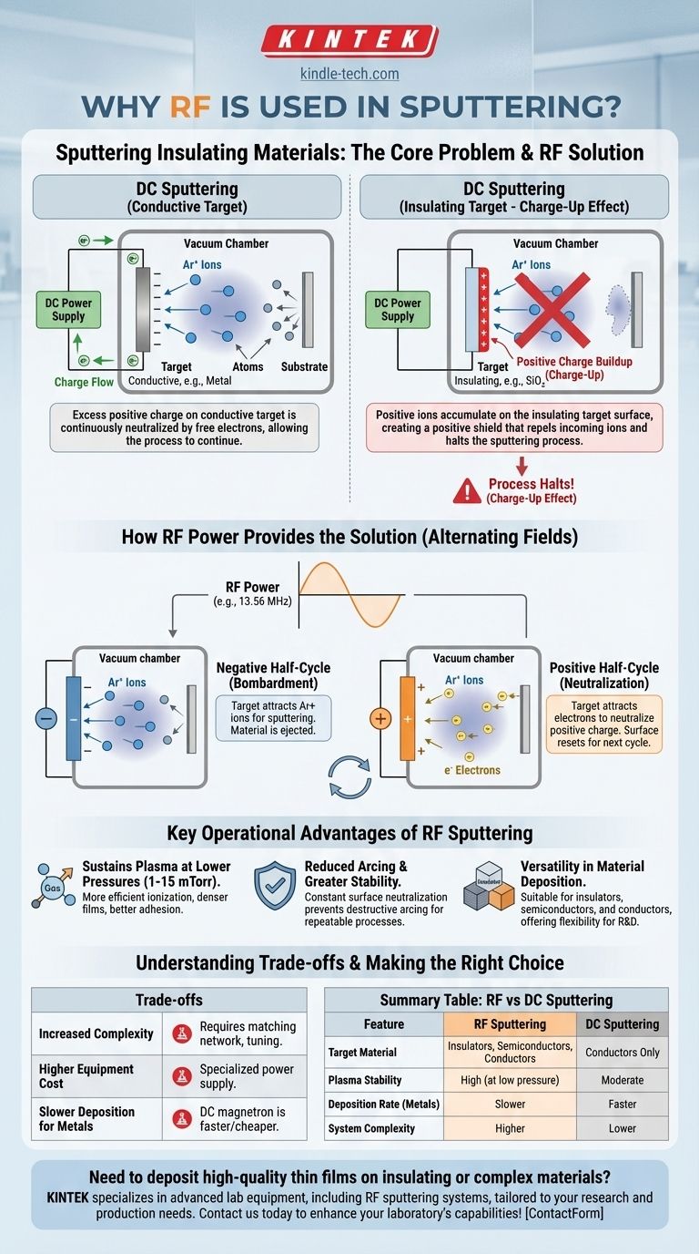
The Core Problem: Sputtering Insulating Materials
To understand the value of RF, we must first look at the fundamental challenge of sputtering insulators with a direct current.
The 'Charge-Up' Effect in DC Sputtering
In any sputtering process, positively charged gas ions (like Argon, Ar+) are accelerated towards a negatively charged target.
When these ions strike a conductive target, the excess positive charge is immediately neutralized by the free electrons within the metal and conducted away through the power supply.
However, when ions strike an insulating target, the positive charge cannot flow away. This charge accumulates on the target's surface, creating a positive shield that repels the incoming positive ions and effectively kills the sputtering process.
How RF Power Provides the Solution
RF power solves this problem by rapidly alternating the voltage on the target, typically at a frequency of 13.56 MHz. This creates two distinct half-cycles.
In the negative half-cycle, the target is negatively biased, attracting positive ions from the plasma to bombard the surface and sputter material, just as intended.
In the positive half-cycle, the target becomes positively biased. It now attracts highly mobile electrons from the plasma, which flood the surface and neutralize the positive charge built up during the previous cycle. Because electrons are much lighter and more mobile than ions, this neutralization happens very quickly, preparing the surface for the next bombardment cycle.
Key Operational Advantages of RF Sputtering
Beyond its ability to handle insulators, the use of an RF source brings several other process benefits.
Sustaining Plasma at Lower Pressures
RF power is more efficient at ionizing the process gas than a simple DC field. This allows a stable plasma to be maintained at much lower pressures (e.g., 1-15 mTorr).
Operating at lower pressure reduces the chance that sputtered atoms will collide with gas atoms on their way to the substrate. This leads to a more direct deposition path, resulting in denser, higher-quality films with better adhesion.
Reduced Arcing and Greater Stability
The constant neutralization of surface charge prevents the massive potential differences that can lead to destructive arcing. This makes the overall process far more stable and repeatable, which is critical for manufacturing complex devices.
Versatility in Material Deposition
An RF power supply can be used to sputter any type of material, including insulators, semiconductors, and conductors. While DC might be faster for metals, an RF system provides the ultimate flexibility for research and development environments where many different materials are used.
Understanding the Trade-offs
While powerful, RF sputtering is not always the default choice due to several important considerations.
Increased System Complexity
RF systems require a specialized, high-cost power supply and, critically, an impedance matching network. This network is necessary to efficiently transfer power from the supply to the plasma. Tuning this network adds a layer of complexity to process setup and control.
Higher Equipment Cost
An RF power supply and its associated matching network are significantly more expensive than a standard DC power supply. This capital investment is a primary consideration for any production line.
Slower Deposition Rates for Metals
For purely conductive materials, DC magnetron sputtering almost always offers higher deposition rates and lower cost than RF sputtering. The efficiency of the DC process for metals is difficult for RF to match, making DC the preferred method for metallization.
Making the Right Choice for Your Process
Your choice between RF and other sputtering techniques should be driven entirely by the material you need to deposit and your process priorities.
- If your primary focus is depositing insulating or dielectric materials (like SiO₂, Al₂O₃, or PZT): RF sputtering is the necessary and standard industry solution.
- If your primary focus is depositing conductive materials (like aluminum, copper, or gold) at high speed: DC magnetron sputtering is the more efficient and cost-effective choice.
- If your primary focus is research and development with a wide variety of materials: An RF system offers the greatest versatility, as it can sputter insulators, semiconductors, and conductors.
Ultimately, understanding the role of RF power transforms sputtering from a single method into a versatile toolkit, allowing you to select the right energy source for the specific material you need to deposit.
Summary Table:
| Feature | RF Sputtering | DC Sputtering |
|---|---|---|
| Target Material | Insulators, Semiconductors, Conductors | Conductors Only |
| Plasma Stability | High (at low pressure) | Moderate |
| Deposition Rate for Metals | Slower | Faster |
| System Complexity | Higher (requires matching network) | Lower |
| Cost | Higher | Lower |
Need to deposit high-quality thin films on insulating or complex materials? KINTEK specializes in advanced lab equipment, including RF sputtering systems, to help you achieve precise, stable, and versatile deposition results. Our solutions are tailored to meet the demands of research and production environments. Contact us today to discuss how our expertise can enhance your laboratory's capabilities!
Visual Guide
Related Products
- RF PECVD System Radio Frequency Plasma-Enhanced Chemical Vapor Deposition RF PECVD
- Spark Plasma Sintering Furnace SPS Furnace
- Horizontal High Temperature Graphite Vacuum Graphitization Furnace
People Also Ask
- What is plasma enhanced chemical vapour deposition process? Unlock Low-Temperature, High-Quality Thin Films
- What is plasma CVD? Unlock Low-Temperature Thin Film Deposition for Sensitive Materials
- How does plasma enhance CVD? Unlock Low-Temperature, High-Quality Film Deposition
- What is plasma chemical vapor deposition? A Low-Temperature Thin Film Coating Solution
- What is plasma enhanced chemical Vapour deposition process used for fabrication of? A Guide to Low-Temperature Thin Films


