Sputter coating is a sample preparation technique used to apply a very thin, electrically conductive layer onto a non-conductive specimen. This process is essential for imaging these materials in a Scanning Electron Microscope (SEM) without distorting the image.
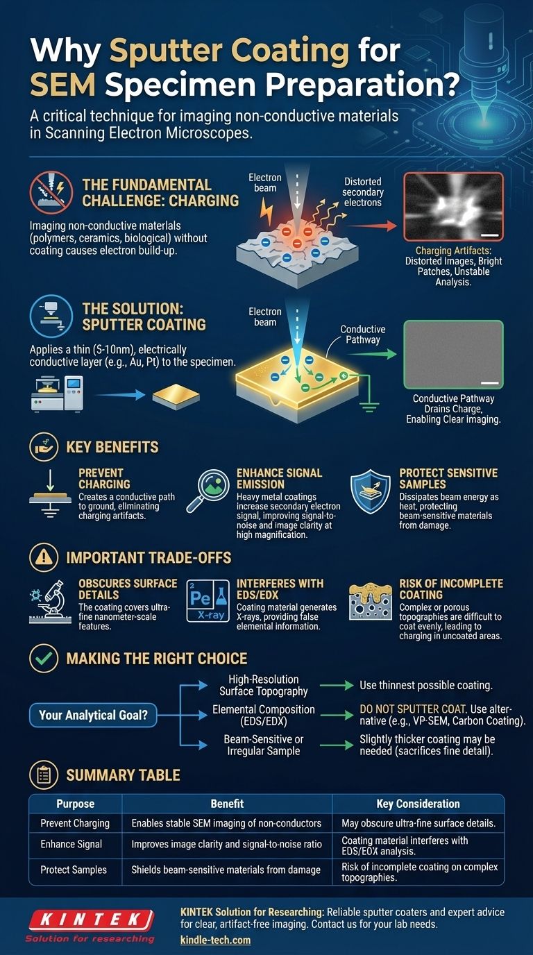
The core problem with imaging non-conductive materials in an SEM is "charging," where electrons from the microscope's beam accumulate on the surface and ruin the image. Sputter coating solves this by creating a conductive pathway that drains this charge away, enabling clear and stable analysis.

The Fundamental Challenge: Imaging Non-Conductive Materials
To understand why sputter coating is necessary, you must first understand the basic physics of a Scanning Electron Microscope.
Why SEMs Require Conductivity
An SEM works by scanning a focused beam of high-energy electrons across a specimen's surface. The interactions between these electrons and the sample generate various signals, primarily secondary electrons, which are then collected to form an image.
For this process to work correctly, the electrons from the beam must have a path to travel off the sample and into an electrical ground. On a conductive material like metal, this happens automatically.
The Problem of "Charging"
On a non-conductive or insulating material (like a polymer, ceramic, or biological sample), there is no path to ground. The electrons from the beam become trapped on the surface, causing a rapid build-up of negative charge.
This phenomenon, known as charging, is highly detrimental to SEM imaging. The accumulated negative field deflects the incoming electron beam and pushes away the secondary electrons trying to leave the surface.
The Visual Impact of Charging Artifacts
Charging artifacts ruin SEM images in predictable ways. They often appear as abnormally bright patches, streaks, or distorted lines that obscure the true surface topography.
In severe cases, the image can become completely unstable, flickering or shifting as the charge builds and discharges unpredictably, making any meaningful analysis impossible.
How Sputter Coating Provides the Solution
Sputter coating directly counteracts the problem of charging by fundamentally altering the electrical properties of the specimen's surface.
Creating a Conductive Pathway
The sputter coater deposits a thin film of conductive material, typically gold, platinum, or a gold-palladium alloy, across the entire sample. This layer is usually only 5 to 10 nanometers thick.
This ultrathin metal film acts as a conductive highway, connecting every point on the sample's surface to the SEM's grounded specimen holder. It provides a path for incoming electrons to dissipate, preventing any charge build-up.
Enhancing Signal Emission
In addition to preventing charging, the metallic coating can also improve image quality. Heavy metals like gold and platinum are very efficient at emitting secondary electrons when struck by the electron beam.
This leads to a stronger signal and a higher signal-to-noise ratio, resulting in sharper, clearer images, especially at high magnification.
Protecting Sensitive Samples
For delicate specimens like biological tissue or soft polymers, the electron beam can cause damage. The metallic coating helps to dissipate the beam's energy as heat and electrical charge, offering a degree of protection to the underlying beam-sensitive material.
Understanding the Trade-offs of Sputter Coating
While essential, sputter coating is an additive process with inherent compromises that you must consider.
Obscuring Surface Details
The coating, though incredibly thin, is not infinitesimal. It will cover the absolute finest surface features. If your goal is to resolve details on the scale of just a few nanometers, the coating itself may obscure what you are trying to see.
Loss of Compositional Information
If you plan to perform elemental analysis using Energy-Dispersive X-ray Spectroscopy (EDS or EDX), sputter coating is a major problem. The X-rays generated will come from the coating material, not the underlying sample, leading to false elemental information.
The Risk of Incomplete Coating
Specimens with complex, porous, or highly irregular topography are difficult to coat evenly. Any uncoated areas can still suffer from charging. Achieving a uniform layer on such samples requires meticulous technique, often using a rotary-planetary specimen stage to expose all surfaces to the coating source.
Making the Right Choice for Your Analysis
Your analytical goal should dictate your approach to sample preparation.
- If your primary focus is high-resolution surface topography of a non-conductor: Sputter coating is essential, but use the thinnest possible coating that prevents charging to preserve detail.
- If your primary focus is elemental composition (EDS/EDX): Do not sputter coat. You must use an alternative like a variable pressure/environmental SEM (VP-SEM) or carbon coating, which produces a much weaker interfering signal.
- If your sample is beam-sensitive or highly irregular: A slightly thicker coating may be needed for protection and to ensure complete coverage, but be aware this will sacrifice some fine surface detail.
By understanding these principles, you can use sputter coating as a precise tool to enable analysis, not just a routine step, ensuring the integrity and accuracy of your results.
Summary Table:
| Purpose | Benefit | Key Consideration |
|---|---|---|
| Prevent Charging | Enables stable SEM imaging of non-conductors | May obscure ultra-fine surface details |
| Enhance Signal | Improves image clarity and signal-to-noise ratio | Coating material interferes with EDS/EDX analysis |
| Protect Samples | Shields beam-sensitive materials from damage | Risk of incomplete coating on complex topographies |
Need to optimize your SEM sample preparation? KINTEK specializes in lab equipment and consumables, providing reliable sputter coaters and expert advice to help you achieve clear, artifact-free imaging. Whether you're working with polymers, ceramics, or biological samples, our solutions ensure your non-conductive specimens are prepared correctly for accurate analysis. Contact us today to discuss your laboratory needs and enhance your imaging results!
Visual Guide
Related Products
People Also Ask
- Why is Chemical Vapor Deposition (CVD) equipment uniquely suited for constructing hierarchical superhydrophobic structures?
- What is the hot filament chemical vapour deposition of diamond? A Guide to Synthetic Diamond Coating
- What is the full form of HFCVD? A Guide to Hot Filament Chemical Vapor Deposition
- What are the advantages of chemical vapor deposition? Achieve Superior Thin Films for Your Lab
- What is the specific function of the metal filament in HF-CVD? Key Roles in Diamond Growth
