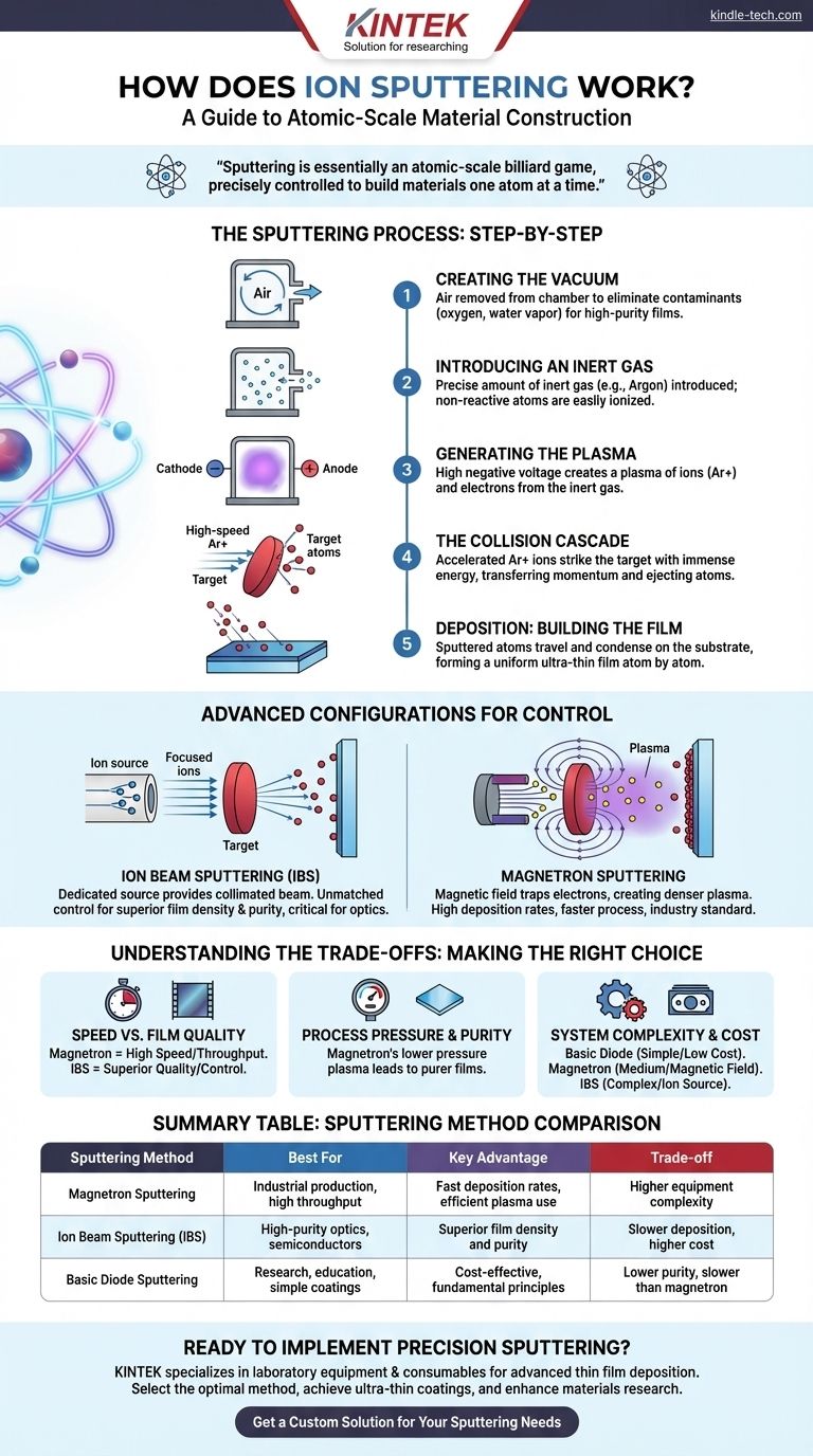
At its core, ion sputtering is a physical vapor deposition (PVD) technique that uses high-energy ions to knock atoms off a source material, known as a target. These dislodged atoms then travel through a vacuum and deposit onto a substrate, forming an ultra-thin, highly uniform film. It is essentially an atomic-scale billiard game, precisely controlled to build materials one atom at a time.
Sputtering is not merely a method for moving atoms; it is a highly controllable engineering process. By manipulating plasma and ion beams within a vacuum, we gain the ability to construct thin films with specific, desirable properties like high density and purity, which are impossible to achieve otherwise.
The Fundamental Sputtering Process: A Step-by-Step Breakdown
To understand how sputtering works, it's best to visualize the sequence of events inside the deposition chamber for a basic configuration.
1. Creating the Environment: The Vacuum
First, both the target (the source material) and the substrate (the surface to be coated) are placed inside a high-vacuum chamber. All air is pumped out to remove contaminants like oxygen and water vapor, which would otherwise react with the sputtered material and compromise the purity of the film.
2. Introducing an Inert Gas
Once a vacuum is established, a small, precisely controlled amount of an inert gas, most commonly Argon (Ar), is introduced. This gas is chosen because it is non-reactive and its atoms can be easily ionized.
3. Generating the Plasma
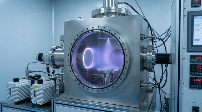
A high negative voltage is applied to the target, making it a cathode. This strong electric field pulls free electrons from the target. These electrons collide with the neutral Argon atoms, knocking an electron off the Argon and creating a positively charged Argon ion (Ar+). This process repeats, creating a self-sustaining cloud of ions and electrons known as a plasma, which often has a characteristic glow.
4. The Collision Cascade
The newly formed, positively charged Argon ions are now strongly accelerated by the electric field toward the negatively charged target. They strike the target surface with immense kinetic energy.
This high-energy impact initiates a collision cascade within the target material. The ion transfers its momentum to the target atoms, which in turn strike other atoms, similar to a break in a game of pool.
5. Deposition: Building the Film
Some of the target atoms near the surface gain enough energy from this cascade to be ejected, or "sputtered," from the target. These sputtered atoms travel in a straight line through the low-pressure environment until they strike the substrate.
Upon arrival, they condense on the cooler substrate, gradually building up a thin film atom by atom.
Advanced Sputtering Configurations for Control
While the basic process is effective, several advanced configurations have been developed to enhance efficiency, quality, and speed.
Ion Beam Sputtering (IBS)
In Ion Beam Sputtering, the plasma generation is physically separated from the target. A dedicated ion source creates a highly focused, collimated beam of monoenergetic ions. This beam is then aimed directly at the target.
This separation provides unmatched control over the ion energy and angle of incidence, resulting in films with superior density and purity, crucial for high-performance optics and electronics.
Magnetron Sputtering
Magnetron sputtering is the most common industrial method. It adds a powerful magnetic field near the target surface. This field traps the free electrons from the plasma, forcing them to travel in a spiral path close to the target.
This confinement dramatically increases the probability that an electron will collide with and ionize an Argon atom. The result is a much denser plasma and a significantly higher sputtering rate, allowing the process to run faster and at lower pressures.
Understanding the Trade-offs
Choosing a sputtering method involves balancing competing priorities. There is no single "best" technique; the optimal choice depends entirely on the goal.
Speed vs. Film Quality
Magnetron sputtering is significantly faster than other methods, making it ideal for industrial-scale production where throughput is critical.
Ion Beam Sputtering, by contrast, is much slower but offers unparalleled control over film properties. The resulting films are exceptionally dense and pure, but this quality comes at the cost of time and equipment complexity.
Process Pressure and Purity
A key advantage of magnetron sputtering is its ability to sustain a plasma at lower pressures. Lower pressure means fewer inert gas atoms are present in the chamber, reducing the chance that they become embedded in the growing film as impurities. This leads to purer films compared to basic diode sputtering.
System Complexity and Cost
As control and efficiency increase, so does the complexity and cost of the equipment. A basic diode sputtering system is relatively simple, while a magnetron system requires strong magnets, and an IBS system requires a separate, sophisticated ion source.
Making the Right Choice for Your Goal
Your application's requirements will dictate the most appropriate sputtering method.
- If your primary focus is rapid production and high throughput: Magnetron sputtering is the industry standard, offering excellent deposition rates and high-quality films for a wide range of applications.
- If your primary focus is creating the highest-purity, densest films for demanding applications (e.g., optical coatings, semiconductors): Ion Beam Sputtering (IBS) provides the ultimate level of control needed, despite its slower deposition rate.
- If your primary focus is education, fundamental research, or simple coatings on a budget: A basic DC or RF diode sputtering system is a sufficient and cost-effective starting point for understanding the core principles.
By understanding these principles, you can select the precise atomic-level construction tool for your specific engineering challenge.
Summary Table:
| Sputtering Method | Best For | Key Advantage | Trade-off |
|---|---|---|---|
| Magnetron Sputtering | Industrial production, high throughput | Fast deposition rates, efficient plasma use | Higher equipment complexity |
| Ion Beam Sputtering (IBS) | High-purity optics, semiconductors | Superior film density and purity | Slower deposition, higher cost |
| Basic Diode Sputtering | Research, education, simple coatings | Cost-effective, fundamental principles | Lower purity, slower than magnetron |
Ready to Implement Precision Sputtering in Your Lab?
KINTEK specializes in laboratory equipment and consumables for advanced thin film deposition. Whether you're developing next-generation semiconductors, optical coatings, or electronic components, our sputtering solutions deliver the precision and control your research demands.
We help you:
- Select the optimal sputtering method for your specific application
- Achieve ultra-thin, uniform coatings with exceptional purity
- Enhance your materials research with reliable, high-performance equipment
Contact our experts today to discuss how our sputtering systems can advance your laboratory capabilities.
Get a Custom Solution for Your Sputtering Needs
Visual Guide
Related Products
- Spark Plasma Sintering Furnace SPS Furnace
- Chemical Vapor Deposition CVD Equipment System Chamber Slide PECVD Tube Furnace with Liquid Gasifier PECVD Machine
- RF PECVD System Radio Frequency Plasma-Enhanced Chemical Vapor Deposition RF PECVD
- Customer Made Versatile CVD Tube Furnace Chemical Vapor Deposition Chamber System Equipment
- Vacuum Induction Melting Spinning System Arc Melting Furnace
People Also Ask
- What are the advantages of CAMI/SPS for W-Cu composite preparation? Reduce cycles from hours to seconds.
- What is the mechanism of SPS process? A Deep Dive into Rapid, Low-Temperature Sintering
- What are the fundamentals of spark plasma sintering process? Unlock Rapid, High-Performance Material Consolidation
- What is the difference between spark plasma sintering and flash sintering? A Guide to Advanced Sintering Methods
- What is the pressure for spark plasma sintering? A Guide to Optimizing SPS Parameters


