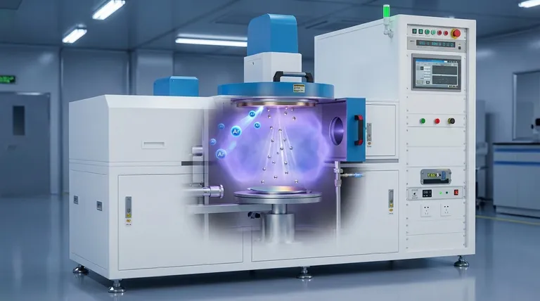
At its core, sputtering is a physical process used to deposit exceptionally thin and uniform layers of material onto a surface. It works by creating a plasma in a vacuum and using energized ions from this plasma to physically knock atoms off a source material, known as the "target." These dislodged atoms then travel and coat a destination object, or "substrate," forming a highly controlled thin film.
Sputtering is not simply "spraying" atoms. It is a highly controlled vacuum deposition technique where an inert gas is ionized to create a plasma. These ions are then accelerated to bombard a target, dislodging atoms through physical momentum transfer, which then deposit onto a substrate to form a precise thin film.
The Anatomy of the Sputtering Process
To understand how sputtering works, you must first recognize its key components, which operate in a carefully controlled environment.
The Vacuum Chamber
The entire process takes place inside a sealed vacuum chamber. Removing air and other reactive gases is critical to prevent contamination of the film and to allow the sputtered atoms to travel freely from the target to the substrate.
The Target
The target is a solid slab of the material you wish to deposit. It acts as the source for the thin film. A high-voltage negative charge is applied to the target, making it a cathode.
The Substrate
This is the object or material that will be coated. It is strategically placed to intercept the stream of atoms ejected from the target.
The Sputtering Gas
An inert gas, most commonly Argon (Ar), is introduced into the chamber at a very low pressure. This gas is not part of the final film; instead, it serves as the "ammunition" for the bombardment process.
The Sputtering Mechanism, Step-by-Step
The process unfolds in a precise sequence, transforming a solid target into an atomic vapor that builds a new film.
Step 1: Creating the Plasma
After introducing the Argon gas, a strong electric field is applied. Free electrons in the chamber are accelerated by this field and collide with the neutral Argon atoms, knocking an electron off the Argon atom.
This creates a positively charged Argon ion (Ar+) and another free electron, which can then ionize more Argon atoms. This chain reaction sustains a glowing, energized state of matter known as a plasma—a mix of positive ions, electrons, and neutral atoms.
Step 2: Ion Bombardment
The positively charged Argon ions (Ar+) are strongly attracted to the negatively charged target. They accelerate toward the target at high velocity, gaining significant kinetic energy.
Step 3: Atomic Ejection via Momentum Transfer
When these high-energy ions strike the target surface, they transfer their momentum to the target atoms in a process similar to a billiard ball collision. This initial impact sets off a collision cascade within the first few atomic layers of the target material.
If this cascade directs enough energy back toward the surface—an amount greater than the material's surface binding energy—a target atom is physically knocked loose and ejected from the surface. This ejected atom is what we call "sputtered."
Step 4: Deposition and Film Growth
The sputtered atoms travel in a straight line through the vacuum until they strike the substrate. Upon arrival, they stick to the surface (a process called adsorption) and begin to build up, layer by layer.
Over time, this accumulation of atoms forms a continuous, dense, and highly adherent thin film on the substrate's surface.
Understanding the Trade-offs and Control Factors
The final properties of the sputtered film are not accidental; they are a direct result of controlling key process parameters. Understanding these trade-offs is essential for achieving the desired outcome.
Gas Pressure
Lowering the gas pressure reduces the chance of sputtered atoms colliding with gas atoms on their way to the substrate. This results in a denser, higher-quality film but often decreases the deposition rate. Conversely, higher pressure can increase the deposition rate but may lead to more porous films.
Target Power and Voltage
Increasing the voltage (and thus the power) applied to the target increases the energy of the bombarding ions. This boosts the sputter yield—the number of atoms ejected per incoming ion—resulting in a faster deposition rate. However, excessive power can cause unwanted heating of the substrate and target.
Choice of Gas
The mass of the inert gas ion affects the efficiency of momentum transfer. Heavier gases like Krypton (Kr) or Xenon (Xe) are more efficient at sputtering heavy target materials than Argon, leading to higher deposition rates. However, they are also significantly more expensive.
System Geometry
The distance and orientation between the target and the substrate have a major impact on film uniformity and thickness. A shorter distance can increase the rate but may reduce uniformity across a large substrate.
Applying This to Your Goal
The versatility of sputtering comes from your ability to tune these parameters to achieve a specific result.
- If your primary focus is a high deposition rate: Increase the power applied to the target and consider using a heavier inert gas like Krypton to maximize momentum transfer.
- If your primary focus is film quality and density: Use a lower gas pressure to ensure the sputtered atoms travel a clear path and maintain precise control over substrate temperature.
- If your primary focus is coating a complex alloy: Sputtering is ideal, as the physical ejection mechanism generally preserves the elemental ratios from the target to the film.
- If your primary focus is adhesion: Sputtering provides excellent film adhesion because the arriving atoms have enough energy to embed slightly into the substrate surface, creating a strong bond.
By mastering these core principles, you can leverage sputtering to engineer surfaces with specific optical, electrical, or mechanical properties at the atomic level.
Summary Table:
| Key Component | Role in the Sputtering Process |
|---|---|
| Vacuum Chamber | Provides a contamination-free environment for atom travel. |
| Target (Cathode) | Source material that is bombarded to release coating atoms. |
| Substrate | The object or surface that receives the thin film coating. |
| Sputtering Gas (e.g., Argon) | Ionized to create plasma for bombarding the target. |
| Plasma | A mix of ions and electrons that energizes the sputtering process. |
Ready to engineer surfaces with precision thin films? KINTEK specializes in lab equipment and consumables for sputtering and other deposition techniques. Our expertise helps laboratories achieve superior film adhesion, density, and uniformity. Whether you're developing semiconductors, optical coatings, or advanced materials, we provide the reliable equipment and support you need. Contact our experts today to discuss your specific application and discover how KINTEK can enhance your R&D or production capabilities.
Visual Guide
