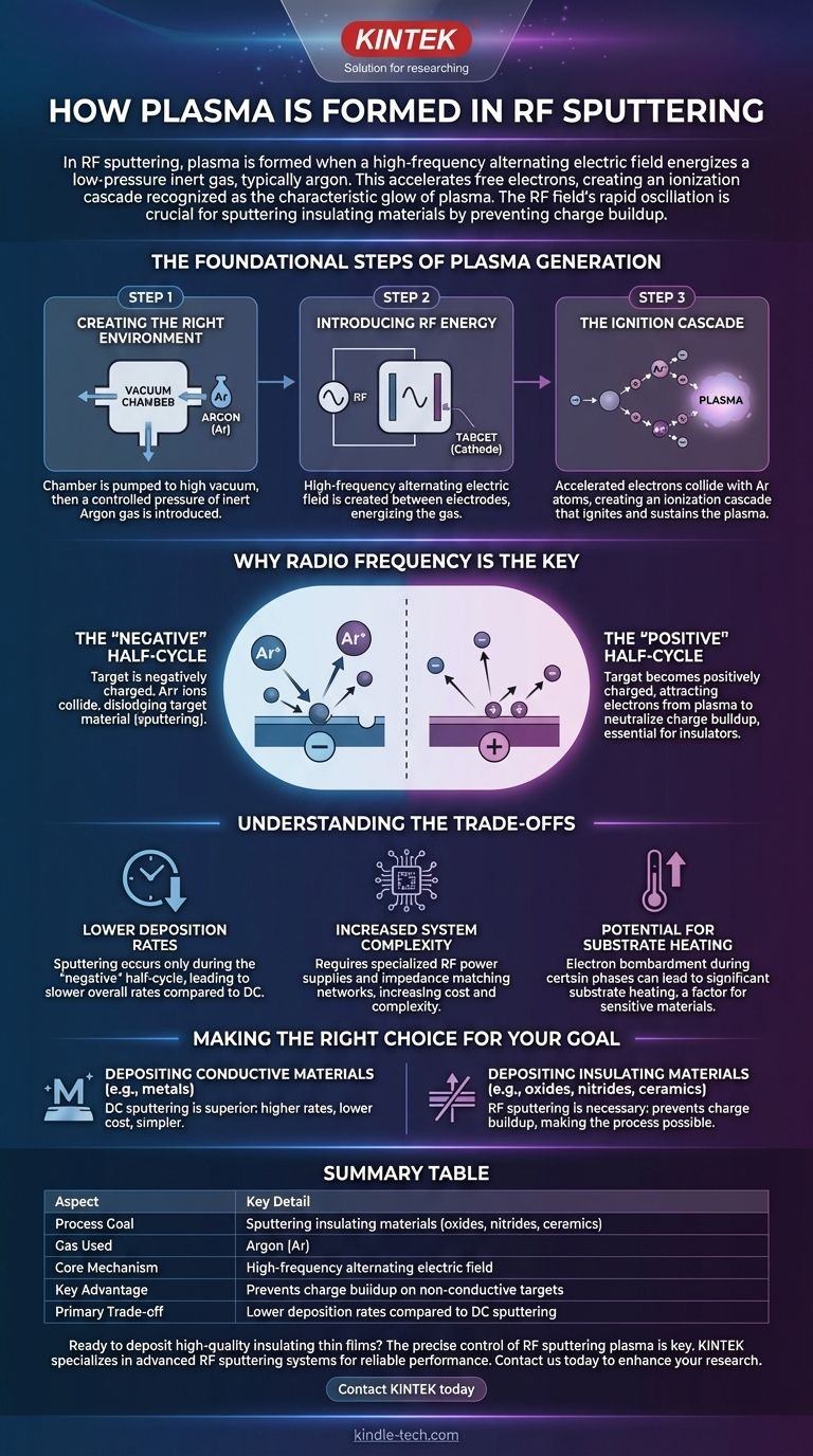
In RF sputtering, plasma is formed when a high-frequency alternating electric field energizes a low-pressure inert gas, typically argon. This powerful field accelerates free electrons, causing them to collide with and strip electrons from the gas atoms. This process creates a self-sustaining cascade of positive ions and electrons, which we recognize as the characteristic glow of plasma.
The core principle is not just creating the plasma, but using the rapid oscillation of the Radio Frequency (RF) field to overcome the primary challenge of sputtering insulating materials. The alternating field prevents a fatal buildup of electrical charge on the target surface, which would otherwise halt the process.
The Foundational Steps of Plasma Generation
Before sputtering can occur, the system must create the precise conditions necessary to ignite and sustain a plasma. This process happens in a few distinct stages inside a vacuum chamber.
Creating the Right Environment
First, the chamber is pumped down to a high vacuum to remove air and other contaminants. An inert gas, most commonly argon (Ar), is then introduced into the chamber at a very low, controlled pressure. This gas provides the atoms that will be converted into the plasma.
Introducing RF Energy
An RF power source is activated, creating a high-frequency, alternating electric field between two electrodes. The material to be deposited, known as the target, is placed on one electrode (the cathode).
The Ignition Cascade
Within the argon gas, there are always a few stray free electrons. The alternating electric field grabs these electrons and accelerates them rapidly back and forth. As these energized electrons collide with neutral argon atoms, they knock additional electrons loose.
This action creates positively charged argon ions (Ar+) and more free electrons, which are then accelerated by the field to cause even more collisions. This chain reaction, known as an ionization cascade, is what ignites and sustains the plasma.
Why Radio Frequency is the Key
While a direct current (DC) field can create a plasma, the use of a radio frequency is a specific solution to a difficult problem: sputtering materials that do not conduct electricity.
The "Negative" Half-Cycle
During the half of the RF cycle when the target has a negative voltage, it behaves like a standard DC sputtering system. The large, positive argon ions are accelerated from the plasma and forcefully collide with the target surface, dislodging or "sputtering" atoms of the target material.
The "Positive" Half-Cycle
This is the critical difference. During the other half of the cycle, the target becomes positively charged. Instead of repelling electrons, it attracts them from the plasma. This brief influx of electrons effectively neutralizes any positive charge that has built up on the surface of an insulating target from the previous cycle's ion bombardment.
Preventing Charge Buildup
Without this alternating cycle, sputtering an insulator like an oxide or nitride would cause an immediate buildup of positive charge on the target surface. This charge would repel any incoming argon ions, quickly extinguishing the plasma and stopping the sputtering process entirely. The RF field's rapid switching prevents this from happening.
Understanding the Trade-offs
While essential for certain materials, the RF method is not without its compromises compared to the simpler DC sputtering process.
Lower Deposition Rates
Because the target is only being bombarded with ions during the "negative" half of the cycle, the overall rate at which material is sputtered is typically lower than with DC sputtering, where the bombardment is continuous.
Increased System Complexity
RF power systems are inherently more complex and expensive than their DC counterparts. They require a specialized RF power supply and an impedance matching network to efficiently transfer power into the plasma.
Potential for Substrate Heating
The electron bombardment of the substrate during certain phases of the RF cycle can lead to more significant substrate heating than is typically seen in DC sputtering. This can be a critical factor when working with heat-sensitive materials.
Making the Right Choice for Your Goal
The decision between RF and DC sputtering is determined entirely by the electrical properties of your target material.
- If your primary focus is depositing conductive materials (e.g., metals): DC sputtering is almost always the superior choice due to its higher deposition rates, lower cost, and simpler operation.
- If your primary focus is depositing insulating materials (e.g., oxides, nitrides, ceramics): RF sputtering is the necessary and correct method, as it is specifically designed to prevent the charge buildup that makes DC sputtering impossible.
Ultimately, understanding how the RF field interacts with the plasma empowers you to select the precise tool required for your specific thin-film deposition needs.
Summary Table:
| Aspect | Key Detail |
|---|---|
| Process Goal | Sputtering insulating materials (oxides, nitrides, ceramics) |
| Gas Used | Argon (Ar) |
| Core Mechanism | High-frequency alternating electric field |
| Key Advantage | Prevents charge buildup on non-conductive targets |
| Primary Trade-off | Lower deposition rates compared to DC sputtering |
Ready to deposit high-quality insulating thin films? The precise control of RF sputtering plasma is key to your success. At KINTEK, we specialize in advanced lab equipment, including RF sputtering systems designed for reliable performance with a wide range of target materials. Let our experts help you configure the perfect solution for your laboratory's specific research and production goals.
Contact KINTEK today to discuss your project and discover how our expertise can enhance your thin-film deposition process.
Visual Guide
Related Products
- RF PECVD System Radio Frequency Plasma-Enhanced Chemical Vapor Deposition RF PECVD
- Horizontal High Temperature Graphite Vacuum Graphitization Furnace
- Spark Plasma Sintering Furnace SPS Furnace
- Automatic Laboratory Hydraulic Press for XRF & KBR Pellet Press
- Electron Beam Evaporation Coating Oxygen-Free Copper Crucible and Evaporation Boat
People Also Ask
- What is plasma CVD? Unlock Low-Temperature Thin Film Deposition for Sensitive Materials
- How does Radio Frequency Enhanced Plasma Chemical Vapour Deposition (RF-PECVD) work? Learn the Core Principles
- What is plasma enhanced chemical vapour deposition PECVD used for? Enable Low-Temp Thin Films for Electronics & Solar
- What is plasma enhanced chemical vapour deposition process? Unlock Low-Temperature, High-Quality Thin Films
- What is an example of PECVD? RF-PECVD for High-Quality Thin Film Deposition


