Characterizing single-walled carbon nanotubes (SWCNTs) requires a suite of analytical techniques, as no single method can reveal all their properties. This process involves determining their structural integrity, purity, and, most importantly, their electronic and optical characteristics, which are defined by their specific atomic structure (chirality). The primary methods employed are microscopy for direct visualization and spectroscopy for probing their unique vibrational and electronic "fingerprints."
A complete characterization of an SWCNT sample is never achieved with a single instrument. It requires a complementary approach, typically combining microscopy (like TEM) for structural validation with spectroscopy (like Raman) for a statistical, bulk assessment of quality and type.
Structural Characterization: Visualizing the Nanotube
The first step in characterization is often to confirm that you have, in fact, produced nanotubes with the correct morphology. This is the domain of high-resolution microscopy.
Transmission Electron Microscopy (TEM)
TEM is the gold standard for direct structural analysis. It provides high-magnification images that allow you to visualize individual nanotubes.
With TEM, you can directly measure a nanotube's diameter and length. Crucially, it is the most definitive method for confirming that the tubes are single-walled.
Scanning Electron Microscopy (SEM)
SEM offers a lower-resolution view compared to TEM. It is not used for analyzing individual tubes but is essential for assessing the bulk morphology of the sample.
This technique reveals how the nanotubes are arranged on a larger scale—whether they form bundles, tangled networks (often called "buckypaper"), or aligned arrays.
Atomic Force Microscopy (AFM)
AFM scans a surface with a tiny physical probe to create a 3D topographical map. It provides extremely precise height measurements.
For SWCNTs deposited on a flat substrate, AFM is an excellent tool for accurately measuring diameter and observing the dispersion and aggregation of individual tubes.
Spectroscopic Characterization: Probing Intrinsic Properties
While microscopy shows you what the nanotubes look like, spectroscopy tells you what they are by probing their quantum mechanical properties. This is critical for understanding their electronic behavior.
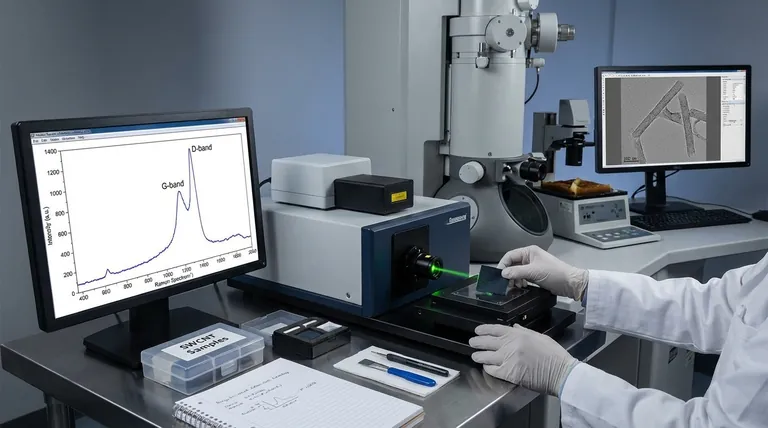
Raman Spectroscopy: The Fingerprint of an SWCNT
Raman spectroscopy is arguably the most powerful and common technique for SWCNT characterization. It is fast, non-destructive, and incredibly sensitive to the nanotube's atomic structure.
Key features in the Raman spectrum include:
- Radial Breathing Mode (RBM): A low-frequency peak whose position is inversely proportional to the nanotube's diameter. This feature is a definitive sign of SWCNTs.
- D-band: This peak indicates the presence of defects, such as broken carbon bonds or amorphous carbon.
- G-band: This peak confirms the presence of graphitic sp²-hybridized carbon, the fundamental structure of a nanotube wall. The ratio of the G-band to D-band intensity (G/D) is a primary measure of nanotube quality and purity.
UV-Vis-NIR Absorption Spectroscopy
SWCNTs absorb light at specific wavelengths depending on their diameter and chirality. This creates a unique absorption spectrum in the ultraviolet, visible, and near-infrared (UV-Vis-NIR) range.
The spectrum shows distinct peaks corresponding to electronic transitions. These peaks allow you to determine the distribution of different nanotube species in a bulk sample and to differentiate between semiconducting and metallic tubes.
Photoluminescence (PL) Spectroscopy
Only semiconducting SWCNTs exhibit photoluminescence (fluorescence), a property where they absorb light at one wavelength and emit it at a longer one.
By creating a 2D map of emission intensity versus excitation wavelength, PL spectroscopy generates a detailed "chirality map." This map acts as a unique fingerprint, identifying the exact (n,m) indices of the semiconducting species present in the sample.
Understanding the Trade-offs
Choosing the right characterization technique involves understanding the limitations and purpose of each method. There is no single "best" tool.
Microscopy vs. Spectroscopy
Microscopy provides direct, unambiguous images but suffers from poor statistics. An image of a few perfect nanotubes in TEM does not mean the entire batch is high quality.
Spectroscopy provides statistically significant, bulk-averaged data about the entire sample. However, the information is indirect and requires careful interpretation.
The Challenge of Impurities
A major goal of characterization is to quantify purity. Common impurities include amorphous carbon (detected by the D-band in Raman) and residual metal catalyst particles from synthesis (often visible in TEM).
Techniques like thermogravimetric analysis (TGA), which measures weight loss upon heating, are also used to quantify the amount of carbon versus non-combustible metal catalysts.
Making the Right Choice for Your Goal
Your characterization strategy should be dictated by your end goal.
- If your primary focus is confirming successful synthesis and basic quality: Start with Raman spectroscopy to check for the RBM peak and a high G/D intensity ratio.
- If your primary focus is determining the distribution of electronic types: Use UV-Vis-NIR absorption for a rapid, bulk assessment of the metallic and semiconducting populations.
- If your primary focus is performing detailed structural validation on individual tubes: Use Transmission Electron Microscopy (TEM) for direct imaging of diameter, length, and wall structure.
- If your primary focus is identifying the exact chirality of semiconducting tubes for optical applications: Photoluminescence (PL) spectroscopy is the most powerful and specific tool.
An effective characterization plan always combines multiple, complementary techniques to build a complete and reliable picture of your material.
Summary Table:
| Technique | Primary Purpose | Key Information Provided |
|---|---|---|
| TEM | Structural Validation | Direct imaging of diameter, length, and single-walled structure |
| Raman Spectroscopy | Quality & Purity Assessment | RBM peak (diameter), G/D ratio (quality), D-band (defects) |
| UV-Vis-NIR Absorption | Electronic Type Distribution | Identifies semiconducting vs. metallic SWCNTs in bulk samples |
| Photoluminescence (PL) | Chirality Mapping | Fingerprints exact (n,m) indices of semiconducting SWCNTs |
| SEM/AFM | Bulk Morphology & Dispersion | Assesses nanotube arrangement, bundles, and surface distribution |
Ready to unlock the full potential of your SWCNT research?
Accurate characterization is the foundation of successful nanotechnology development. KINTEK specializes in providing the high-quality lab equipment and consumables you need for precise SWCNT analysis. Whether you're setting up a new lab or optimizing your current workflows, our experts can help you select the right tools—from Raman spectrometers to TEM sample preparation supplies—to ensure reliable, reproducible results.
Contact our team today to discuss your specific application needs and discover how KINTEK can support your laboratory's success. Get in touch with our experts now!
Visual Guide

Related Products
- Laboratory CVD Boron Doped Diamond Materials
- Hydrophilic Carbon Paper TGPH060 for Battery Lab Applications
- Professional Cutting Tools for Carbon Paper Cloth Diaphragm Copper Aluminum Foil and More
- Conductive Carbon Cloth Carbon Paper Carbon Felt for Electrodes and Batteries
- Multifunctional Electrolytic Electrochemical Cell Water Bath Single Layer Double Layer
People Also Ask
- Are CVD diamonds synthetic? Discover the Truth About Lab-Grown Diamonds
- What is the demand of CVD diamonds? Driven by Ethics, Purity, and Affordability
- How much cheaper are CVD diamonds? Save 20-30% on a Genuine Diamond
- What are the advantages of BDD electrodes? Maximize Wastewater Treatment Efficiency and Durability
- Are CVD diamonds good? Real Diamonds with Ethical Origins & Better Value