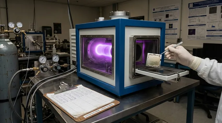
While sputter deposition is a cornerstone of modern thin film technology, it is not without significant drawbacks. The primary disadvantages are its relatively slow deposition speed compared to methods like evaporation, its process complexity requiring expensive equipment, and inherent risks to material integrity, such as film contamination and potential substrate damage from ion bombardment.
Sputtering exchanges speed and simplicity for precision and versatility. Its core disadvantages—slower rates, higher costs, and potential for material damage—are the direct trade-offs for achieving the dense, uniform, and highly controlled films that other methods often cannot produce.
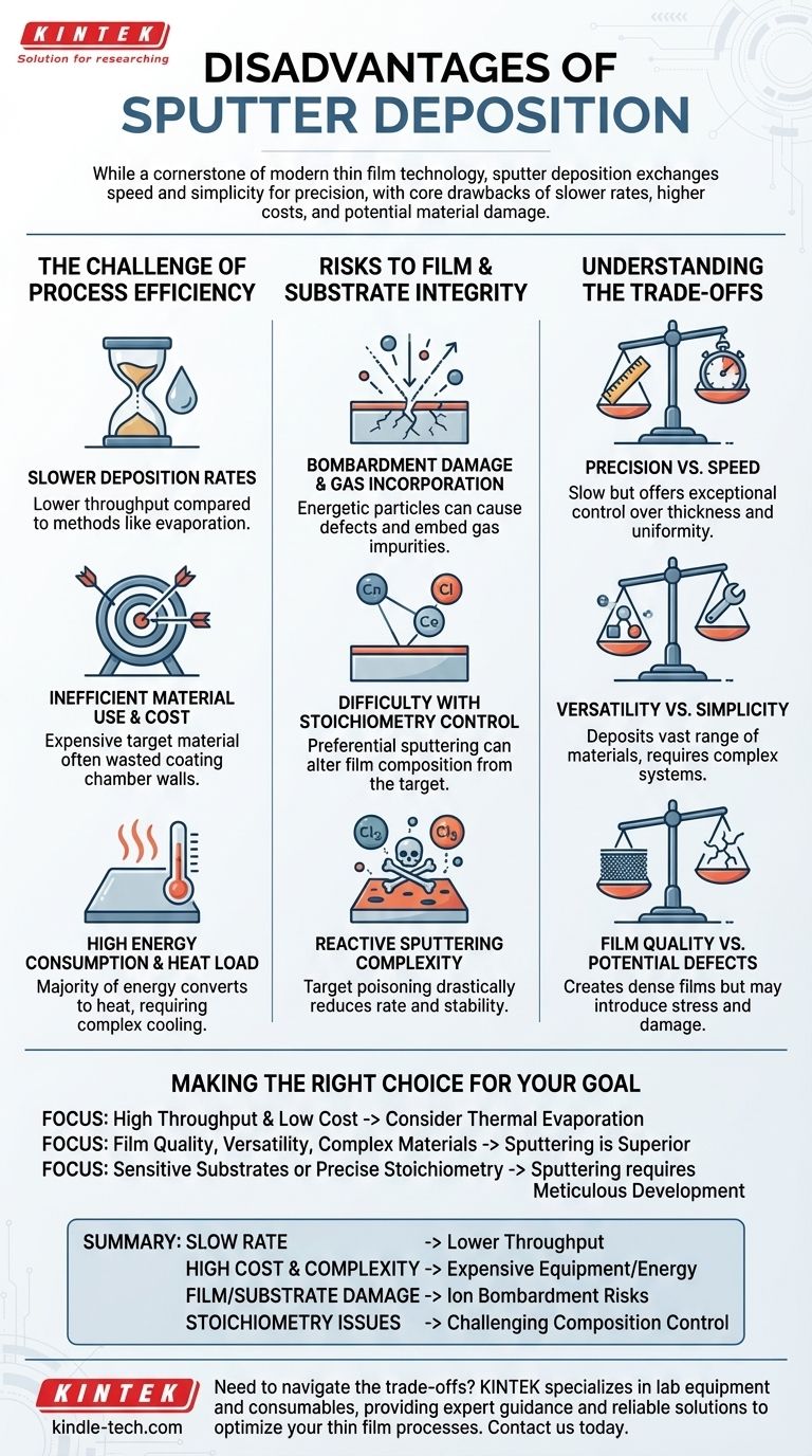
The Challenge of Process Efficiency
Sputter deposition is a highly controlled but often inefficient process. The fundamental physics of ejecting atoms one by one from a target using ion bombardment introduces limitations in speed, cost, and energy consumption.
Slower Deposition Rates
Compared to thermal evaporation, where material is rapidly boiled off, sputtering is a much slower, atom-by-atom removal process. This results in lower deposition rates, which can be a bottleneck in high-volume manufacturing environments.
Inefficient Material Use and Cost
The sputtering target, which is often made of expensive, high-purity material, is a significant operational cost. Sputtered atoms are ejected in various directions, coating not only the substrate but also the chamber walls and fixtures, leading to poor material utilization.
High Energy Consumption and Heat Load
The vast majority of the energy from the bombarding ions is converted into heat at the target, not into kinetic energy for the sputtered atoms. This immense heat load must be actively managed with complex cooling systems to prevent target damage and maintain process stability.
Risks to Film and Substrate Integrity
The energetic nature of the sputtering process, while beneficial for creating dense films, also carries risks. The plasma environment and ion bombardment can introduce unintended defects or alter the material's fundamental properties.
Bombardment Damage and Gas Incorporation
The energetic particles within the plasma can cause radiation or bombardment damage, especially to sensitive substrates or the growing film itself. Furthermore, atoms from the plasma gas (typically Argon) can become embedded in the film, creating impurities that alter its electrical, optical, or mechanical properties.
Difficulty with Stoichiometry Control
When sputtering compound materials or alloys, one element may be sputtered more readily than another (a phenomenon called preferential sputtering). This can cause the composition of the deposited film to differ from the composition of the target, making precise stoichiometry control a significant challenge.
Reactive Sputtering Complexity
Introducing a reactive gas (like oxygen or nitrogen) to create oxide or nitride films requires extremely careful control. If not managed properly, the target surface itself can become coated with the compound—a condition known as target poisoning—which drastically reduces the deposition rate and process stability.
Understanding the Trade-offs
No deposition technique is perfect. The disadvantages of sputtering must be weighed against its unique advantages, making it an engineering choice based on specific project goals.
Precision vs. Speed
Sputtering is slow, but it provides exceptional control over film thickness and uniformity across large areas, especially when substrate rotation is used. Methods like thermal evaporation are faster but offer far less control over film structure and consistency.
Versatility vs. Simplicity
Sputtering is highly versatile. It can deposit a vast range of materials, including alloys and insulators (using RF power supplies), that are impossible to deposit via thermal evaporation. This versatility comes at the cost of more complex and expensive vacuum systems, power supplies, and gas handling.
Film Quality vs. Potential Defects
The same energetic bombardment that creates dense, strongly adherent films can also introduce stress, gas incorporation, and substrate damage. Achieving high-quality films requires a careful balancing act, optimizing process parameters to maximize the benefits while minimizing the drawbacks.
Making the Right Choice for Your Goal
Selecting a deposition method requires aligning the process capabilities with your primary objective.
- If your primary focus is high throughput and low cost for simple metals: Thermal evaporation may be a more efficient choice, provided you can tolerate its limitations in uniformity and material choice.
- If your primary focus is film quality, material versatility, or depositing complex materials: Sputtering is often the superior method, as long as you can accommodate the higher initial cost and process complexity.
- If you are working with sensitive substrates or require precise stoichiometry: Sputtering is viable, but it demands meticulous process development to mitigate damage and control the final film composition.
Understanding these limitations is the first step toward leveraging sputter deposition's unique strengths for your specific application.
Summary Table:
| Disadvantage | Key Impact |
|---|---|
| Slow Deposition Rate | Lower throughput compared to evaporation methods. |
| High Cost & Complexity | Expensive targets, equipment, and high energy consumption. |
| Risk of Film/Substrate Damage | Ion bombardment can cause defects and gas incorporation. |
| Difficulty with Stoichiometry | Challenging to control composition for alloys/compounds. |
Need to navigate the trade-offs of thin film deposition for your laboratory? KINTEK specializes in lab equipment and consumables, providing expert guidance and reliable solutions for sputtering and other deposition techniques. Our team can help you select the right equipment to balance film quality, cost, and throughput for your specific research or production goals. Contact us today to optimize your thin film processes!
Visual Guide
Related Products
- Chemical Vapor Deposition CVD Equipment System Chamber Slide PECVD Tube Furnace with Liquid Gasifier PECVD Machine
- RF PECVD System Radio Frequency Plasma-Enhanced Chemical Vapor Deposition RF PECVD
- Tungsten Evaporation Boat for Thin Film Deposition
- Custom CVD Diamond Coating for Lab Applications
- HFCVD Machine System Equipment for Drawing Die Nano-Diamond Coating
People Also Ask
- What are the advantages of chemical vapor deposition? Achieve Superior Thin Films for Your Lab
- What is the chemical vapor deposition growth process? Build Superior Thin Films from the Atom Up
- What is plasma enhanced chemical vapor deposition PECVD equipment? A Guide to Low-Temperature Thin Film Deposition
- Why is Chemical Vapor Deposition (CVD) equipment uniquely suited for constructing hierarchical superhydrophobic structures?
- What are the core advantages of PE-CVD in OLED encapsulation? Protect Sensitive Layers with Low-Temp Film Deposition


