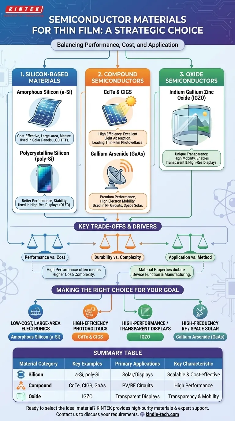
In short, the primary semiconductor materials used for thin films are not a single group but fall into three main categories: silicon-based materials, compound semiconductors like Cadmium Telluride (CdTe) and Copper Indium Gallium Selenide (CIGS), and emerging oxide semiconductors. These materials are chosen based on their specific electronic properties, suitability for a given application like a solar cell or display, and compatibility with a deposition method.
The selection of a thin-film semiconductor material is never about finding a single "best" option. It is a strategic engineering decision that balances the required electronic performance, manufacturing cost and complexity, and the final application's unique demands.
The Core Categories of Thin-Film Semiconductors
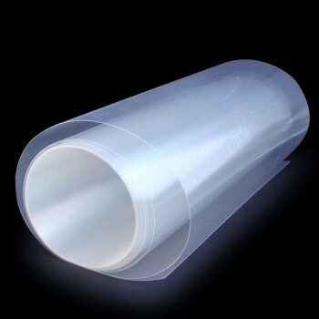
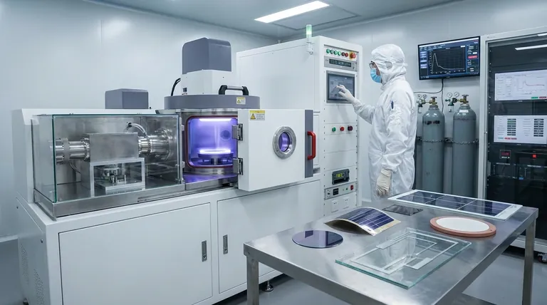
While many materials can be deposited as a thin film, only certain ones possess the semiconductor properties needed for electronic devices. They are generally sourced in high-purity forms, such as sputtering targets or precursor gases, for controlled deposition.
Silicon (Amorphous and Polycrystalline)
Silicon is the foundational material of the entire semiconductor industry. In thin-film applications, it is most often used in two main forms.
Amorphous Silicon (a-Si) lacks a crystalline structure, which makes it cheaper to deposit over large areas. It's a workhorse for applications where cost is more critical than peak performance, such as in solar panels and the thin-film transistors (TFTs) that control LCD screen pixels.
Polycrystalline Silicon (poly-Si) consists of many small silicon crystals. It offers better electronic performance and stability than a-Si, making it a preferred choice for higher-resolution displays like OLEDs, where faster transistor switching speeds are necessary.
Compound Semiconductors
These materials are formed from two or more elements to achieve specific properties that silicon cannot.
Cadmium Telluride (CdTe) and Copper Indium Gallium Selenide (CIGS) are leading materials in the thin-film photovoltaic industry. They are highly efficient at converting sunlight into electricity, often outperforming silicon in certain conditions.
Gallium Arsenide (GaAs) is another key compound semiconductor. While more expensive, it offers exceptionally high electron mobility, making it ideal for high-frequency applications like RF circuits in mobile phones and high-efficiency solar cells for space applications.
Oxide Semiconductors
A newer class of materials, oxide semiconductors are gaining significant traction for their unique properties, particularly transparency.
These are often amorphous heavy-metal cation multicomponent oxides, such as Indium Gallium Zinc Oxide (IGZO). Their ability to be both electrically conductive (as a semiconductor) and optically transparent makes them essential for creating transparent transistors used in modern high-resolution and transparent displays.
How Material Choice Drives Application
The material is not chosen in isolation. Its properties are intrinsically linked to the intended device, the manufacturing method, and the required performance.
Linking Material to Function
The unique benefits of each material class steer their use. CdTe and CIGS are dominant in solar cells because of their excellent light absorption. IGZO is used in displays because it allows for the creation of invisible circuits on a glass panel.
The Role of Deposition Method
The choice of material is also constrained by the available manufacturing processes. Methods like Chemical Vapor Deposition (CVD) require volatile precursor gases, while sputtering uses a solid target.
A material like CIGS, with its four elements, requires highly sophisticated co-evaporation or sputtering techniques to ensure the correct chemical composition across the film. This adds manufacturing complexity compared to depositing a single-element material like silicon.
Understanding the Trade-offs
Every material choice involves compromises. Being aware of these is critical for making sound engineering and business decisions.
Performance vs. Cost
There is a direct trade-off between device performance and manufacturing cost. High-performance materials like Gallium Arsenide are significantly more expensive to synthesize and deposit than amorphous silicon. This is why a-Si is used for large, cost-sensitive solar farms, while GaAs is reserved for niche, high-value applications.
Durability vs. Mechanical Properties
Material properties extend beyond the electronic. The references note that some oxides can be brittle, which can be a limiting factor for flexible electronics. This contrasts with certain polymer-based organic semiconductors (a separate category), which offer superior flexibility but often have lower performance and longevity.
Manufacturing Complexity
Simpler materials are easier to manage. Depositing a consistent film of amorphous silicon is a mature and reliable process. In contrast, compound semiconductors like CIGS require precise control over multiple material sources simultaneously, increasing the potential for defects that can degrade device performance.
Making the Right Choice for Your Goal
Your application dictates the optimal material. Base your decision on your primary objective.
- If your primary focus is low-cost, large-area electronics: Amorphous silicon (a-Si) provides the most mature, scalable, and cost-effective solution.
- If your primary focus is high-efficiency photovoltaics: Compound semiconductors like CdTe and CIGS are the industry standard for high-performance thin-film solar cells.
- If your primary focus is high-performance displays or transparent electronics: Oxide semiconductors like IGZO are the clear choice for enabling the next generation of transparent and high-resolution devices.
- If your primary focus is high-frequency RF or space-grade solar: Gallium Arsenide (GaAs) remains the premium material for applications demanding the absolute highest electron mobility and efficiency.
Ultimately, selecting the right semiconductor is a careful balancing act between the laws of physics, the realities of manufacturing, and the demands of the market.
Summary Table:
| Material Category | Key Examples | Primary Applications | Key Characteristic |
|---|---|---|---|
| Silicon | Amorphous Silicon (a-Si), Polycrystalline Silicon (poly-Si) | Solar panels, LCD TFTs, OLED displays | Cost-effective, scalable for large areas |
| Compound Semiconductors | Cadmium Telluride (CdTe), CIGS, Gallium Arsenide (GaAs) | High-efficiency solar cells, RF circuits | High performance, excellent light absorption |
| Oxide Semiconductors | Indium Gallium Zinc Oxide (IGZO) | High-resolution & transparent displays | High electron mobility, optical transparency |
Ready to select the ideal thin-film semiconductor material for your project? KINTEK specializes in providing high-purity materials and expert support for your lab's semiconductor and thin-film deposition needs. Whether you're developing advanced solar cells, next-generation displays, or high-frequency electronics, we have the products and knowledge to help you succeed. Contact our experts today to discuss your specific requirements!
Visual Guide
Related Products
- Customizable PTFE Wafer Carriers for Semiconductor and Lab Applications
- Electron Beam Evaporation Coating Oxygen-Free Copper Crucible and Evaporation Boat
- Custom PTFE Wafer Holders for Lab and Semiconductor Processing
- Conductive Carbon Cloth Carbon Paper Carbon Felt for Electrodes and Batteries
- Thin-Layer Spectral Electrolysis Electrochemical Cell
People Also Ask
- Why is PTFE wire used for hanging metal specimens in biodiesel corrosion tests? Ensure Pure Experimental Results
- Are semiconductors thin or thick? Discover the Power of Microscopic Thinness in Modern Electronics
- Why is slender PTFE tubing necessary for flow control in multi-channel catalyst aging? Ensure Equal Gas Distribution
- Why are PTFE containers required for PCT leaching tests? Ensure Chemical Inertness and Analytical Precision
- What are the specific applications of PTFE in micro-batch slug flow systems? Enhance Your Microfluidic Reaction Purity