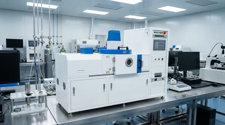
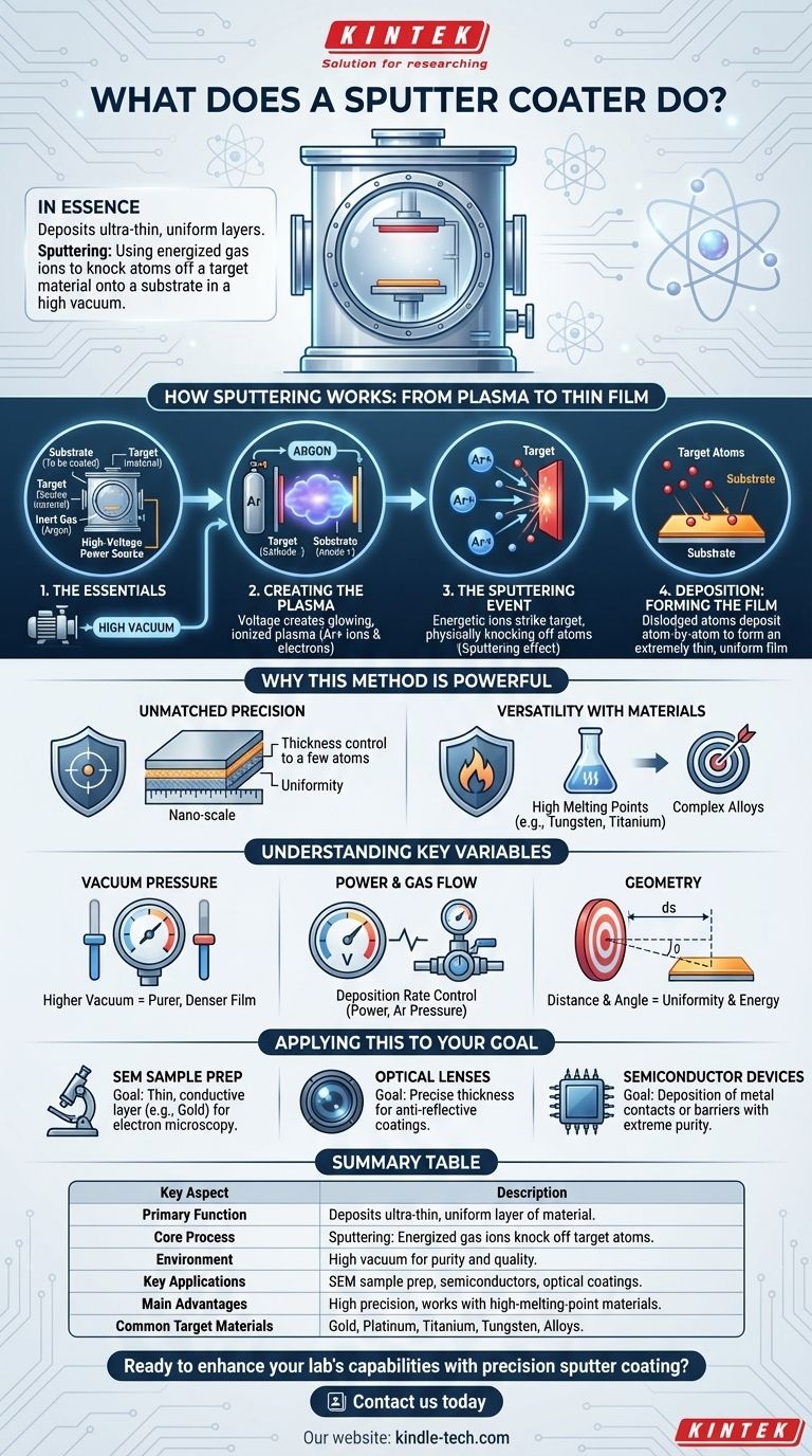
In essence, a sputter coater is a device that deposits an ultra-thin, uniform layer of one material onto the surface of another. This process, known as sputtering, takes place in a high vacuum and is used to create highly precise coatings for applications ranging from semiconductor manufacturing to preparing samples for electron microscopy.
Sputter coating is best understood as a highly controlled, atomic-level collision. It uses energized gas ions as microscopic projectiles to chip atoms off a source material (the "target") and deposit them as a fine, even film onto a sample (the "substrate").
How Sputtering Works: From Plasma to Thin Film
The entire process occurs within a sealed vacuum chamber, which is critical for ensuring the purity and quality of the final coating. The mechanism can be broken down into a few key steps.
The Essential Ingredients
First, four components are required: a substrate (the object to be coated), a target (the material you want to coat with), an inert gas (typically Argon), and a high-voltage power source.
The vacuum is crucial because it removes air and other contaminants that could interfere with the process or become trapped in the thin film.
Creating the Plasma
Once a high vacuum is achieved, a small amount of inert gas, like Argon, is introduced into the chamber. A high voltage is then applied between the target (cathode) and the substrate holder (anode).
This intense electric field energizes the Argon gas, stripping electrons from the atoms and creating a glowing, ionized gas known as plasma. This plasma consists of positively charged Argon ions and free electrons.
The Sputtering Event
The positively charged Argon ions are forcefully accelerated toward the negatively charged target material. Think of these ions as a subatomic form of sandblasting.
Upon impact, the energetic ions physically knock atoms loose from the target's surface. This ejection of target atoms is the "sputtering" effect.
Deposition: Forming the Film
The dislodged atoms from the target travel through the vacuum chamber and land on the surface of the substrate.
Because this is happening on an atom-by-atom basis, the atoms build up into an extremely thin, uniform, and consistent film, coating the substrate evenly.
Why This Method is So Powerful
Sputtering isn't the only way to create a thin film, but its unique characteristics make it indispensable for high-performance applications.
Unmatched Precision
The process allows for an exceptionally high degree of control over the thickness and uniformity of the coating, making it possible to create films that are just a few atoms thick.
Versatility with Materials
Sputtering is especially effective for depositing materials with very high melting points, like tungsten or titanium, which are difficult or impossible to deposit using thermal evaporation methods. It also works exceptionally well for creating films from complex alloys, preserving the alloy's original composition in the final coating.
Understanding the Key Variables
The quality and characteristics of the sputtered film are not accidental; they are the result of carefully controlling several key process parameters. Changing these variables directly impacts the outcome.
The Role of Vacuum Pressure
The level of vacuum is critical. A higher vacuum means fewer stray gas molecules are present to collide with the sputtered atoms as they travel from the target to the substrate, resulting in a purer, denser film.
The Impact of Power and Gas
The voltage and current applied to the target (the power) and the pressure of the sputtering gas (Argon) directly influence the deposition rate. Higher power generally means more ions are created and they strike the target with more force, increasing the speed at which the film is deposited.
The Geometry of the System
The physical arrangement, such as the distance from the target to the substrate, also plays a significant role. This distance affects the uniformity of the coating and the energy with which the sputtered atoms arrive at the substrate.
Applying This to Your Goal
The specific settings you use on a sputter coater depend entirely on what you need to achieve.
- If your primary focus is preparing a non-conductive sample for an SEM (Scanning Electron Microscope): Your goal is a very thin, uniform conductive layer (like gold or platinum) to prevent charging, so you will prioritize low power and process time to achieve a coating of a few nanometers.
- If your primary focus is manufacturing optical lenses: You will need precise control over film thickness to create anti-reflective coatings, requiring careful calibration of power, pressure, and deposition time.
- If your primary focus is producing semiconductor devices: You will use sputtering to deposit various metal layers that act as electrical contacts or barriers, demanding extreme purity, high vacuum, and repeatable process control.
Ultimately, sputter coating provides a powerful method for engineering surfaces at the atomic level.
Summary Table:
| Key Aspect | Description |
|---|---|
| Primary Function | Deposits an ultra-thin, uniform layer of material onto a substrate |
| Core Process | Sputtering: Using energized gas ions to knock atoms off a target material |
| Environment | High vacuum chamber to ensure purity and quality |
| Key Applications | SEM sample preparation, semiconductor manufacturing, optical coatings |
| Main Advantages | High precision, uniform coatings, works with high-melting-point materials |
| Common Target Materials | Gold, platinum, titanium, tungsten, various alloys |
Ready to enhance your lab's capabilities with precision sputter coating?
KINTEK specializes in high-performance lab equipment and consumables, including sputter coaters designed for applications like SEM sample preparation, semiconductor research, and optical coating development. Our solutions deliver the ultra-thin, uniform coatings your work demands, with the reliability and precision that laboratories count on.
Contact us today to discuss how our sputter coating equipment can meet your specific laboratory needs and help you achieve superior results.
Visual Guide
Related Products
- Custom CVD Diamond Coating for Lab Applications
- HFCVD Machine System Equipment for Drawing Die Nano-Diamond Coating
- Multifunctional Electrolytic Electrochemical Cell Water Bath Single Layer Double Layer
- Professional Cutting Tools for Carbon Paper Cloth Diaphragm Copper Aluminum Foil and More
- Chemical Vapor Deposition CVD Equipment System Chamber Slide PECVD Tube Furnace with Liquid Gasifier PECVD Machine
People Also Ask
- What are the advantages of CVD coating? Superior Hardness and Uniformity for Demanding Applications
- What is CVD coating? Transform Your Material's Surface for Maximum Performance
- What are the different CVD coating? A Guide to Thermal CVD, PECVD, and Specialized Methods
- How thick is CVD diamond coating? Balancing Durability and Stress for Optimal Performance
- What is CVD coated? A Guide to Superior Wear Resistance for Complex Parts


