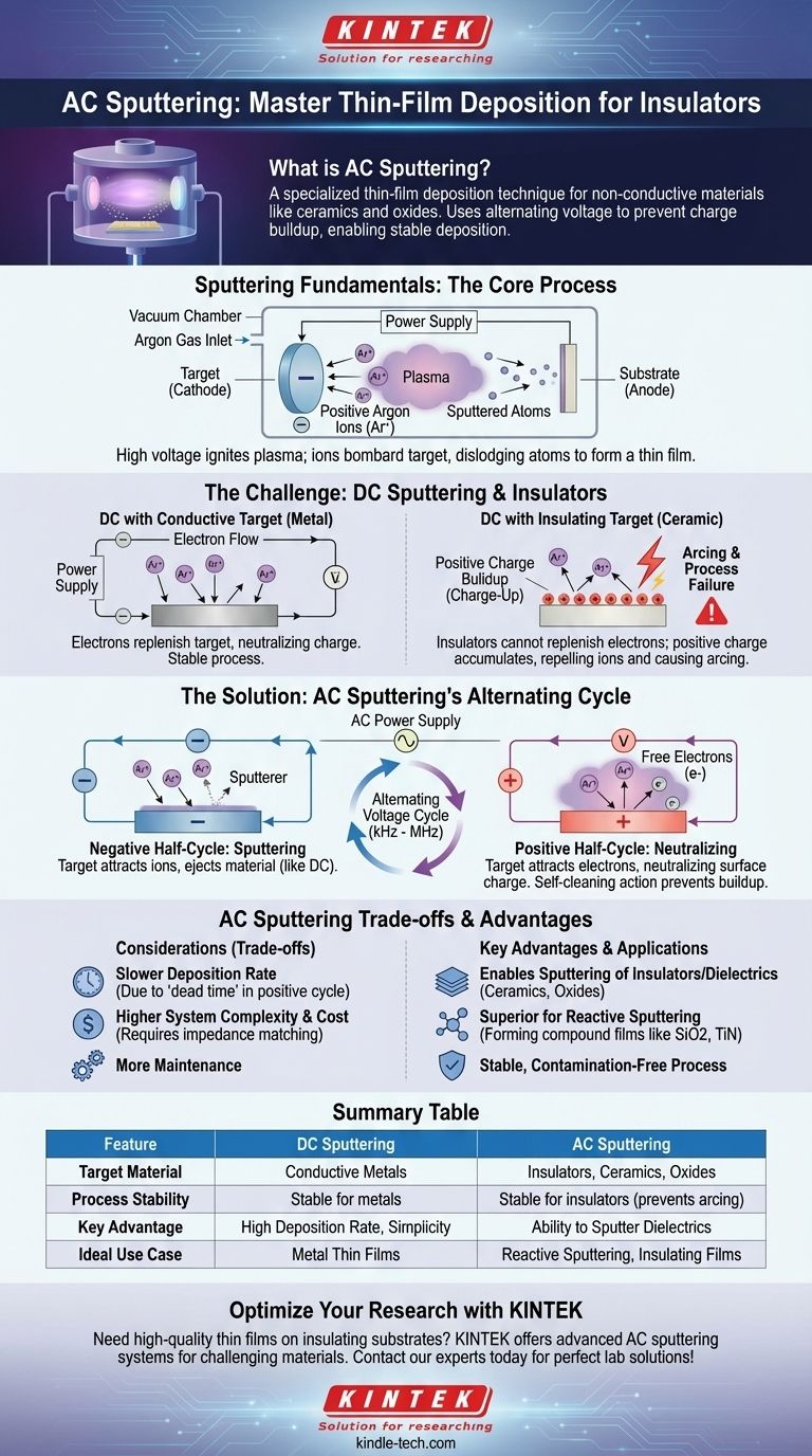
In short, AC sputtering is a specialized thin-film deposition technique used for materials that do not conduct electricity, such as ceramics or oxides. Unlike standard DC sputtering which only works for metals, AC sputtering uses an alternating voltage to prevent a process-killing electrical charge from building up on the insulating target material, enabling stable and continuous deposition.
The core problem with sputtering insulating materials is that they cannot replenish electrons, causing a positive charge to build up that repels the ions needed for sputtering. AC sputtering solves this by rapidly flipping the target's voltage, using one part of the cycle to sputter and the other to attract electrons and neutralize this charge.
The Foundation: Understanding Sputtering Fundamentals
To understand why AC sputtering is necessary, we must first review the basic sputtering process. It is a physical vapor deposition (PVD) method that occurs inside a vacuum chamber.
Creating a Plasma in a Vacuum
The process begins by placing a source material, known as the target, and the item to be coated, the substrate, into a vacuum chamber. The chamber is pumped down to a very low pressure and then backfilled with a small, controlled amount of an inert gas, most commonly argon.
The Bombardment Process
A strong voltage is applied, creating an electric field between the target and the substrate. This voltage ignites the argon gas, stripping electrons from the argon atoms and creating a plasma—a glowing, ionized gas containing positive argon ions and free electrons.
The target is given a strong negative charge, causing it to act as the cathode. This powerfully attracts the positively charged argon ions from the plasma, which accelerate and bombard the target surface with significant kinetic energy.
From Target to Thin Film
This energetic bombardment acts like a sub-atomic sandblaster, dislodging or "sputtering" individual atoms from the target material. These ejected atoms travel through the vacuum chamber and land on the substrate, gradually building up, atom by atom, into a dense and uniform thin film.
The Challenge: Why DC Sputtering Fails with Insulators
The foundational process described above works exceptionally well for electrically conductive targets, like metals. This is known as DC (Direct Current) sputtering because the target maintains a constant negative voltage. However, this method fails completely when the target is an insulator.
The Problem of "Charge-Up"
In DC sputtering, the conductive metal target is connected to the negative terminal of a power supply, allowing it to be a constant source of electrons. When positive argon ions strike the target, the target's conductivity allows it to immediately neutralize that positive charge.
An insulating (or dielectric) target cannot do this. Because it doesn't conduct electricity, it cannot draw electrons from the power supply. When positive argon ions strike the surface and embed themselves, their positive charge accumulates. This phenomenon is known as target poisoning or charge-up.
Arcing and Process Instability
This buildup of positive charge on the target's surface quickly becomes a fatal flaw. The positive surface begins to repel the incoming positive argon ions, effectively shutting down the sputtering process.
Worse, this charge can build to a point where it violently discharges in an uncontrolled arc. This arcing can damage the target, contaminate the substrate, and makes a stable deposition process impossible.
The Solution: How AC Sputtering Works
AC (Alternating Current) sputtering was developed specifically to overcome the charge-up problem on insulating targets. Instead of a constant DC voltage, it uses a power supply that rapidly alternates the target's voltage between negative and positive.
The Alternating Voltage Cycle
The power supply typically operates at a mid-frequency (MF, in the tens of kHz range) or radio frequency (RF, 13.56 MHz). This cycle happens thousands or millions of times per second.
The Negative Half-Cycle: Sputtering the Target
During the brief period when the target is held at a negative voltage, it behaves just like in DC sputtering. It attracts positive argon ions, which bombard the surface and eject target material. During this phase, a small amount of positive charge begins to build up on the surface.
The Positive Half-Cycle: Neutralizing the Charge
Before this charge can become a problem, the voltage flips. During the positive half-cycle, the target briefly becomes positive. It now strongly attracts the free electrons from the plasma. This flood of electrons lands on the target surface, instantly neutralizing the positive charge that built up during the previous negative cycle.
This self-cleaning action ensures the target surface remains electrically neutral on average, preventing charge-up and arcing, and allowing for the continuous, stable sputtering of any material, regardless of its conductivity.
Understanding the Trade-offs
While AC sputtering is a powerful solution, it comes with certain considerations compared to the simpler DC method.
Deposition Rates
Because sputtering only occurs during the negative portion of the AC cycle, the overall deposition rate can be slightly lower than for a DC process running at the same power. The positive cycle is "dead time" for deposition, though it is critical for process stability.
System Complexity and Cost
AC power supplies, particularly RF systems, are significantly more complex and expensive than their DC counterparts. They require impedance matching networks to efficiently transfer power into the plasma, adding another layer of tuning and maintenance.
Reactive Sputtering Superiority
AC sputtering is the superior choice for reactive sputtering. This is a process where a reactive gas (like oxygen or nitrogen) is added to the chamber to form a compound film (e.g., sputtering a silicon target in an oxygen plasma to create silicon dioxide). As the insulating compound forms on the target, AC power prevents it from poisoning the process.
Making the Right Choice for Your Goal
Selecting the correct sputtering method requires understanding the electrical properties of your source material.
- If your primary focus is depositing conductive metals (like gold, copper, or titanium): DC sputtering is the simpler, faster, and more cost-effective choice.
- If your primary focus is depositing insulating materials (like silicon dioxide, aluminum oxide, or other ceramics): AC sputtering (typically RF) is essential to prevent charge buildup and ensure a stable process.
- If your primary focus is creating compound films through reactive sputtering (like titanium nitride or zinc oxide): AC sputtering (often MF or pulsed DC) is the preferred industrial method to manage the formation of insulating layers on the target.
Understanding the fundamental challenge of electrical charge is the key to selecting the correct sputtering technique for your material.
Summary Table:
| Feature | DC Sputtering | AC Sputtering |
|---|---|---|
| Target Material | Conductive Metals | Insulators, Ceramics, Oxides |
| Process Stability | Stable for metals | Stable for insulators (prevents arcing) |
| Key Advantage | High Deposition Rate, Simplicity | Ability to Sputter Dielectrics |
| Ideal Use Case | Metal Thin Films | Reactive Sputtering, Insulating Films |
Need to deposit high-quality thin films on insulating substrates? KINTEK specializes in advanced lab equipment, including AC sputtering systems designed for challenging materials like ceramics and oxides. Our solutions ensure stable, contamination-free deposition for your most demanding research and production goals. Contact our experts today to find the perfect sputtering system for your laboratory's needs!
Visual Guide
Related Products
- Silicon Carbide (SIC) Ceramic Sheet Flat Corrugated Heat Sink for Engineering Advanced Fine Ceramics
- Reference Electrode Calomel Silver Chloride Mercury Sulfate for Laboratory Use
- Spark Plasma Sintering Furnace SPS Furnace
- Boron Nitride (BN) Ceramic Plate
- Professional Cutting Tools for Carbon Paper Cloth Diaphragm Copper Aluminum Foil and More
People Also Ask
- What are the applications of silicon carbide? From Abrasives to High-Tech Semiconductors
- What are the properties and applications of silicon carbide ceramics? Solve Extreme Engineering Challenges
- What is the thermal resistance of SiC? Understanding Its High Thermal Conductivity for Superior Performance
- Why is silicon carbide more efficient? Unlock Higher Power Density with SiC's Superior Material Properties
- What are the common uses of silicon carbide? Unlock Extreme Performance in Harsh Environments