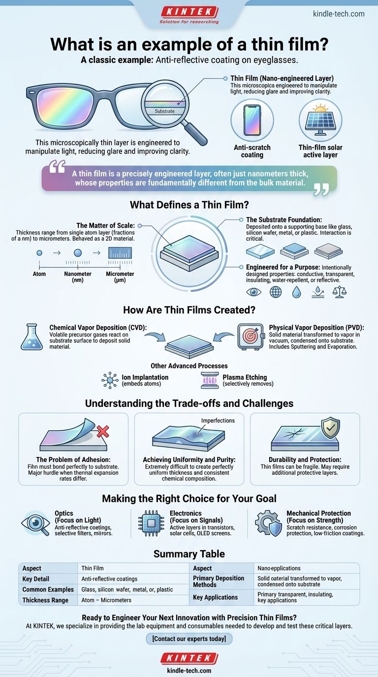
A classic example of a thin film is the anti-reflective coating on a pair of eyeglasses. This microscopically thin layer is engineered to manipulate light, reducing glare and improving clarity. Other common examples include the protective anti-scratch coatings on smartphone screens and the active layers in thin-film solar panels.
A thin film is more than just a small amount of material. It is a precisely engineered layer, often just nanometers thick, whose properties are fundamentally different from the bulk material, making it a critical component in countless modern technologies.
What Defines a Thin Film?
A thin film is a layer of material deposited onto a supporting base, or substrate. Its defining characteristic is its extreme dimensional asymmetry—its thickness is vastly smaller than its length and width.
The Matter of Scale
A thin film’s thickness can range from a single layer of atoms (fractions of a nanometer) up to several micrometers. Because its third dimension (height) is so suppressed, it behaves in many ways like a two-dimensional material.
This extreme thinness is what gives the film unique properties that are not present in the same material in its bulk form.
The Substrate Foundation
Thin films are almost never freestanding; they are deposited onto a substrate. This base can be made of various materials, such as glass, silicon wafers, metal, or plastic, depending on the final application.
The interaction between the film and the substrate is critical for the device's function and durability.
Engineered for a Purpose
The properties of a thin film are not accidental. They are intentionally designed to meet specific application requirements, which can be optical, electronic, mechanical, or chemical.
For instance, a film can be designed to be conductive, transparent, insulating, water-repellent, or reflective to certain wavelengths of light. Often, a single film must meet multiple requirements at once.
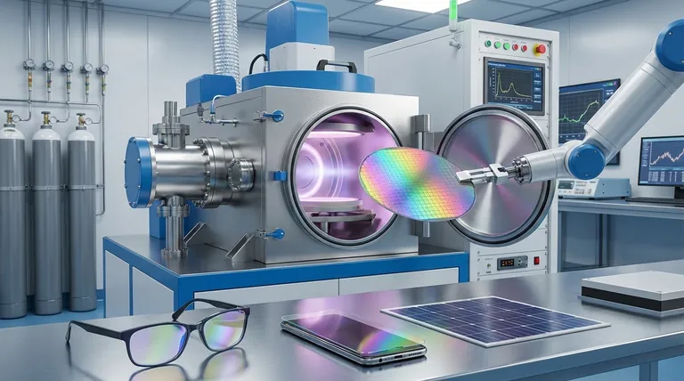
How Are Thin Films Created?
Creating uniform, high-quality thin films requires highly controlled and specialized manufacturing processes. The two primary methods are chemical and physical deposition.
Chemical Vapor Deposition (CVD)
In CVD, the substrate is exposed to volatile precursor gases. A chemical reaction is induced on the substrate's surface, causing a solid material—the thin film—to be deposited.
Physical Vapor Deposition (PVD)
PVD encompasses a set of vacuum deposition methods. It involves physically transforming a solid material into a vapor, transporting it through a vacuum, and condensing it onto the substrate's surface as a thin film. Sputtering and evaporation are common PVD techniques.
Other Advanced Processes
Beyond deposition, other techniques are used to create or modify films. Ion implantation embeds atoms into a surface to change its properties, while plasma etching selectively removes material to create patterns.
Understanding the Trade-offs and Challenges
While incredibly useful, manufacturing and working with thin films present significant engineering challenges that define their limitations and cost.
The Problem of Adhesion
A film is only as good as its bond to the substrate. Ensuring the layer sticks perfectly and permanently without peeling or flaking is a major hurdle, especially when the film and substrate have different thermal expansion rates.
Achieving Uniformity and Purity
Creating a film with a perfectly uniform thickness and consistent chemical composition across an entire surface is extremely difficult. Even microscopic defects or impurities can ruin the performance of an electronic or optical device.
Durability and Protection
By their very nature, thin films can be fragile. A film designed for a specific optical or electronic property may not be mechanically robust, often requiring additional protective layers—which are themselves thin films.
Making the Right Choice for Your Goal
The function of a thin film is dictated entirely by its engineered properties. Its application is a direct result of the problem you need to solve.
- If your primary focus is on optics: You will use thin films as anti-reflective coatings on lenses, selective filters in cameras, or reflective layers in mirrors and displays.
- If your primary focus is on electronics: You will encounter thin films as the fundamental active layers in transistors, the light-absorbing material in solar cells, and the emissive layers in OLED screens.
- If your primary focus is on mechanical protection: You will apply hard, durable thin films to provide scratch resistance for screens, corrosion protection for metals, or low-friction coatings for moving parts.
Ultimately, these microscopic layers are the invisible foundation enabling the performance and durability of the technology we rely on every day.
Summary Table:
| Aspect | Key Detail |
|---|---|
| Common Examples | Anti-reflective coatings on glasses, smartphone screen protectors, thin-film solar panels |
| Thickness Range | Fractions of a nanometer to several micrometers |
| Primary Deposition Methods | Chemical Vapor Deposition (CVD), Physical Vapor Deposition (PVD) |
| Key Applications | Optics (anti-glare), Electronics (solar cells, transistors), Mechanical Protection (scratch resistance) |
Ready to Engineer Your Next Innovation with Precision Thin Films?
Thin films are the foundation of high-performance technology, from advanced optics to durable protective coatings. At KINTEK, we specialize in providing the lab equipment and consumables needed to develop and test these critical layers. Whether you're working on next-generation displays, solar cells, or protective coatings, our solutions help you achieve the uniformity, adhesion, and purity your projects demand.
Let's build the future, one layer at a time. Contact our experts today to discuss your specific laboratory needs!
Visual Guide
Related Products
- Custom CVD Diamond Coating for Lab Applications
- Laboratory CVD Boron Doped Diamond Materials
- Electron Beam Evaporation Coating Oxygen-Free Copper Crucible and Evaporation Boat
- Tungsten Evaporation Boat for Thin Film Deposition
- Molybdenum Tungsten Tantalum Evaporation Boat for High Temperature Applications
People Also Ask
- How thick is CVD diamond coating? Balancing Durability and Stress for Optimal Performance
- What are the different CVD coating? A Guide to Thermal CVD, PECVD, and Specialized Methods
- What is CVD coating? Transform Your Material's Surface for Maximum Performance
- What are the advantages of CVD coating? Superior Hardness and Uniformity for Demanding Applications
- What are the types of CVD coating? A Guide to Choosing the Right Process


