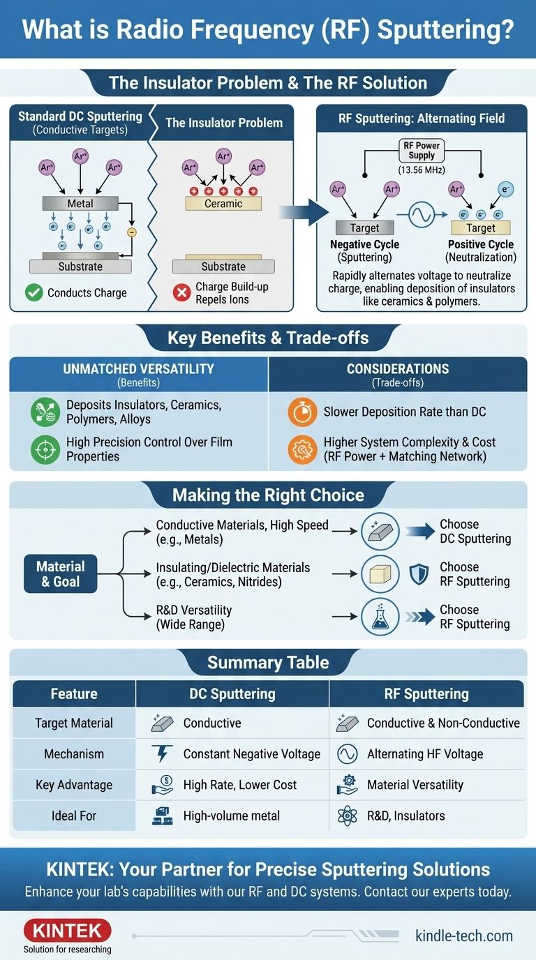
At its core, radio frequency (RF) sputtering is a physical vapor deposition (PVD) technique used to create ultra-thin films of insulating or non-conductive materials. Unlike standard DC sputtering, which only works with conductive targets, RF sputtering uses an alternating electric field to overcome the "charge build-up" effect that otherwise prevents the deposition of materials like ceramics and polymers.
The central challenge in sputtering an insulating material is that it accumulates a positive charge, repelling the very ions needed for the process. RF sputtering solves this by rapidly alternating the voltage, using one part of the cycle to neutralize this charge and the other to continue deposition, thereby enabling a much wider range of materials to be coated.
How Sputtering Fundamentally Works
To understand what makes RF sputtering unique, we must first understand the general sputtering process.
The Basic Mechanism
Sputtering takes place inside a high-vacuum chamber filled with an inert gas, most commonly Argon (Ar). A high voltage is applied to the source material, known as the target, which ignites the gas into a glowing plasma.
This plasma contains positively charged Argon ions (Ar+). These ions are accelerated at high velocity toward the negatively charged target.
The high-energy impact of these ions physically knocks atoms loose from the target's surface. These ejected atoms then travel through the vacuum chamber and deposit onto a substrate (such as a silicon wafer or piece of glass), gradually building up a thin film.
The Goal: A High-Precision Coating
This process allows for extremely precise control over film properties. Engineers can dictate the film's thickness, density, grain structure, and electrical resistivity.
This level of control makes sputtering a critical manufacturing process in industries producing semiconductors, optical lenses, hard drives, and medical implants.
The Insulator Problem RF Sputtering Solves
The simple sputtering mechanism described above works perfectly for conductive targets, but it fails completely with insulators.
The Limitation of DC Sputtering
The standard method, known as DC sputtering, applies a constant negative voltage to the target. This works for metals because they can easily conduct away the positive charge delivered by the arriving Argon ions.
An insulator, by definition, cannot conduct this charge.
The "Charge-Up" Effect
When positive Argon ions strike an insulating target, their positive charge accumulates on the target's surface.
Within moments, this build-up of positive charge becomes so strong that it begins to repel the incoming positive Argon ions. This effectively insulates the target and halts the sputtering process entirely.
The RF Solution: An Alternating Field
RF sputtering overcomes this by replacing the constant DC voltage with a high-frequency alternating voltage, typically at 13.56 MHz.
During the positive half of the AC cycle, a flood of highly mobile electrons from the plasma is attracted to the target, instantly neutralizing the positive charge that built up.
During the negative half of the cycle, the target is again negatively biased, attracting the Argon ions to continue the sputtering process. This rapid switching allows for the continuous deposition of any material, regardless of its conductivity.
Understanding the Trade-offs
While RF sputtering is exceptionally versatile, that capability comes with specific trade-offs compared to the simpler DC method.
Deposition Rate
Because the ion bombardment is effectively paused during the charge-neutralization half of each cycle, RF sputtering is generally slower than DC sputtering. For high-volume production of simple metals, DC is often preferred for its higher throughput.
System Complexity and Cost
An RF sputtering system requires a sophisticated RF power supply and a matching network to efficiently transfer energy into the plasma. This equipment is more complex and expensive than the straightforward power supplies used for DC sputtering.
Unmatched Material Versatility
The primary advantage of RF sputtering is its ability to deposit virtually any material. Oxides, nitrides, ceramics, polymers, and complex alloys can all be deposited with high precision, making it an indispensable tool for advanced materials research and fabrication.
Making the Right Choice for Your Goal
Selecting the correct sputtering method depends entirely on the material you need to deposit and your operational priorities.
- If your primary focus is depositing conductive materials like metals at high speed: Standard DC sputtering is the more efficient and cost-effective choice.
- If your primary focus is depositing insulating or dielectric materials like ceramics (e.g., Al₂O₃) or nitrides (e.g., Si₃N₄): RF sputtering is the essential and correct method to use.
- If your primary focus is versatility for research and development across a wide range of materials: An RF sputtering system offers the broadest capability, able to deposit conductors, semiconductors, and insulators from a single platform.
Ultimately, choosing the right deposition technology is about matching the tool to the specific material challenge at hand.
Summary Table:
| Feature | DC Sputtering | RF Sputtering |
|---|---|---|
| Target Material | Conductive (Metals) | Conductive & Non-Conductive (Ceramics, Polymers) |
| Mechanism | Constant Negative Voltage | Alternating High-Frequency (13.56 MHz) Voltage |
| Key Advantage | High Deposition Rate, Lower Cost | Unmatched Material Versatility |
| Ideal For | High-volume metal coating | R&D and coating insulating materials |
Need to deposit a challenging material?
Whether you are developing next-generation semiconductors, advanced optical coatings, or medical implants, choosing the right deposition technology is critical. KINTEK specializes in lab equipment and consumables, providing the precise sputtering solutions you need for your research and production goals.
Contact our experts today to discuss how our RF and DC sputtering systems can enhance your lab's capabilities and help you achieve superior thin-film results.
Visual Guide
Related Products
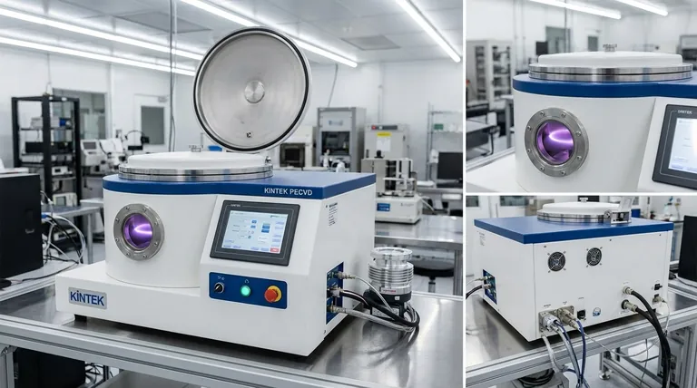
- RF PECVD System Radio Frequency Plasma-Enhanced Chemical Vapor Deposition RF PECVD
- Spark Plasma Sintering Furnace SPS Furnace
- Horizontal High Temperature Graphite Vacuum Graphitization Furnace
People Also Ask
- What is plasma enhanced chemical Vapour deposition process used for fabrication of? A Guide to Low-Temperature Thin Films
- What is plasma enhanced chemical vapour deposition process? Unlock Low-Temperature, High-Quality Thin Films
- How does plasma enhance CVD? Unlock Low-Temperature, High-Quality Film Deposition
- How does Radio Frequency Enhanced Plasma Chemical Vapour Deposition (RF-PECVD) work? Learn the Core Principles
- What is the role of RF-PECVD in VFG preparation? Mastering Vertical Growth and Surface Functionality


