RF (Radio Frequency) sputtering is a physical vapor deposition (PVD) technique used to deposit thin films of insulating or dielectric materials. Unlike standard direct current (DC) sputtering, which only works for conductive targets, RF sputtering applies an alternating voltage. This alternating field prevents the buildup of positive charge on the insulating target surface, a phenomenon that would otherwise repel the bombarding ions and halt the deposition process entirely.
The essential distinction to grasp is that while standard DC sputtering is for conductive materials, RF sputtering is the necessary evolution for depositing non-conductive, insulating materials. It achieves this by using an alternating radio frequency field to continuously neutralize charge buildup on the target's surface.
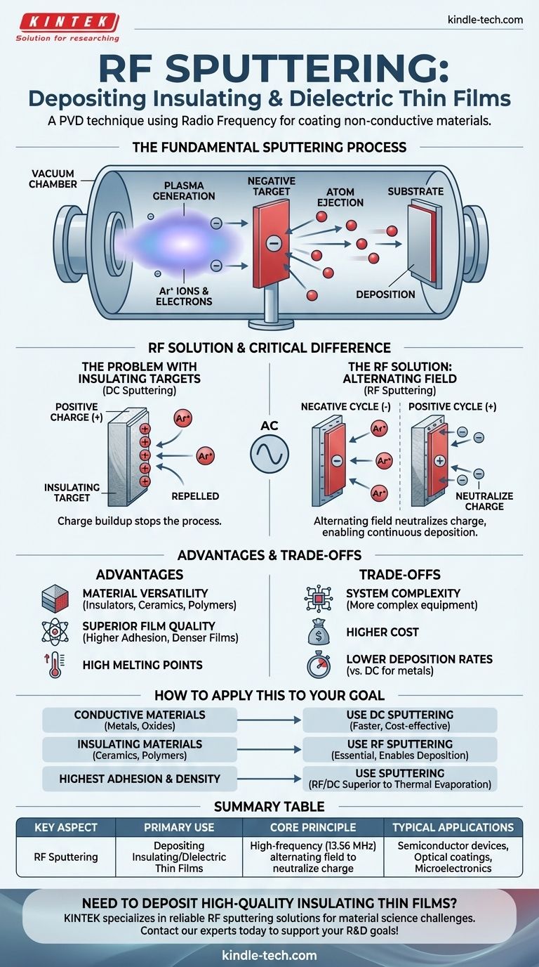
The Fundamental Sputtering Process
To understand why the "RF" component is so crucial, we must first understand the basics of sputtering. It is a vacuum-based process used to create ultra-thin coatings on a substrate.
The Vacuum Chamber
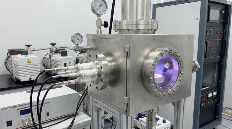
All sputtering occurs within a high-vacuum chamber. This environment removes air and other particles that could contaminate the thin film or interfere with the process.
Plasma Generation
A small amount of an inert gas, typically argon, is introduced into the chamber. An electric field is applied, which strips electrons from the argon atoms, creating a glowing, ionized gas known as a plasma. This plasma consists of positive argon ions and free electrons.
Target Bombardment
A plate of the material to be deposited, known as the target, is given a negative electrical charge. This causes the positively charged argon ions from the plasma to accelerate violently towards the target, bombarding its surface.
Atom Ejection and Deposition
The sheer kinetic energy of these ion collisions is enough to knock atoms loose from the target material. These ejected atoms travel through the vacuum chamber and condense onto a substrate (such as a silicon wafer or piece of glass), gradually building up a thin film.
Why "RF" is the Critical Component
The basic sputtering process described above works perfectly for conductive targets, like metals. However, it fails completely when the target is an electrical insulator.
The Problem with Insulating Targets
If you use a standard DC power source on an insulating target (like a ceramic), the surface immediately accumulates a layer of positive charge from the bombarding argon ions. Because the target cannot conduct this charge away, this positive layer quickly begins to repel any new incoming positive ions, effectively stopping the sputtering process before it can even begin.
The RF Solution: An Alternating Field
RF sputtering solves this by replacing the DC power source with a high-frequency AC source, typically operating at 13.56 MHz. This creates an alternating electrical field with two distinct cycles.
- Negative Cycle: The target becomes negatively charged, attracting the positive argon ions for bombardment and sputtering, just as in the DC process.
- Positive Cycle: The target briefly becomes positively charged. This attracts the free electrons from the plasma, which flood the surface and neutralize the positive ion charge accumulated during the negative cycle.
This rapid switching, happening millions of time per second, effectively tricks the insulating target into behaving like a conductor, allowing for continuous and stable deposition.
Understanding the Advantages and Trade-offs
Sputtering offers unique benefits, and the choice to use an RF source introduces specific considerations.
Material Versatility
This is the primary advantage of RF sputtering. It makes it possible to deposit high-quality films from virtually any material, including metals, alloys, and, most importantly, a vast range of insulators, ceramics, and polymers.
Superior Film Quality
Sputtered atoms have significantly higher kinetic energy than those from thermal evaporation methods. This energy results in denser films with much stronger adhesion to the substrate. Sputtering can also easily deposit materials with extremely high melting points that are difficult to evaporate.
System Complexity and Cost
The main trade-off is complexity. RF power supplies, impedance-matching networks, and shielding are more complex and expensive than their DC counterparts. Deposition rates for RF sputtering can also be lower than for DC sputtering of metals.
How to Apply This to Your Goal
Your choice of deposition method is dictated entirely by the material you need to deposit.
- If your primary focus is depositing conductive materials (metals, conductive oxides): Standard DC sputtering is often the more efficient, faster, and cost-effective choice.
- If your primary focus is depositing insulating materials (ceramics like Al₂O₃, SiO₂, or polymers): RF sputtering is the essential and required technique to successfully create your thin film.
- If your primary focus is achieving the highest adhesion and film density: Sputtering in general (both DC and RF) is a superior choice compared to other methods like thermal evaporation.
Ultimately, RF sputtering is the key that unlocks the deposition of the entire class of non-conductive materials, making it a cornerstone of modern thin-film technology.
Summary Table:
| Key Aspect | RF Sputtering Details |
|---|---|
| Primary Use | Depositing thin films from insulating/dielectric materials (e.g., ceramics, polymers) |
| Core Principle | Uses a high-frequency (13.56 MHz) alternating field to neutralize charge buildup on non-conductive targets |
| Key Advantage | Enables deposition of materials impossible with standard DC sputtering |
| Typical Applications | Semiconductor devices, optical coatings, microelectronics, advanced ceramics |
Need to deposit high-quality insulating thin films? KINTEK specializes in lab equipment and consumables, providing reliable RF sputtering solutions for your laboratory's most demanding material science challenges. Our expertise ensures superior film adhesion and material versatility. Contact our experts today to discuss how we can support your research and development goals!
Visual Guide
Related Products
- RF PECVD System Radio Frequency Plasma-Enhanced Chemical Vapor Deposition RF PECVD
- Spark Plasma Sintering Furnace SPS Furnace
- Horizontal High Temperature Graphite Vacuum Graphitization Furnace
People Also Ask
- What is plasma chemical vapor deposition? A Low-Temperature Thin Film Coating Solution
- What is plasma enhanced chemical vapour deposition process? Unlock Low-Temperature, High-Quality Thin Films
- What is plasma enhanced chemical vapour deposition PECVD used for? Enable Low-Temp Thin Films for Electronics & Solar
- How does plasma enhance CVD? Unlock Low-Temperature, High-Quality Film Deposition
- Why is a Matching Network Indispensable in RF-PECVD for Siloxane Films? Ensure Stable Plasma and Uniform Deposition


