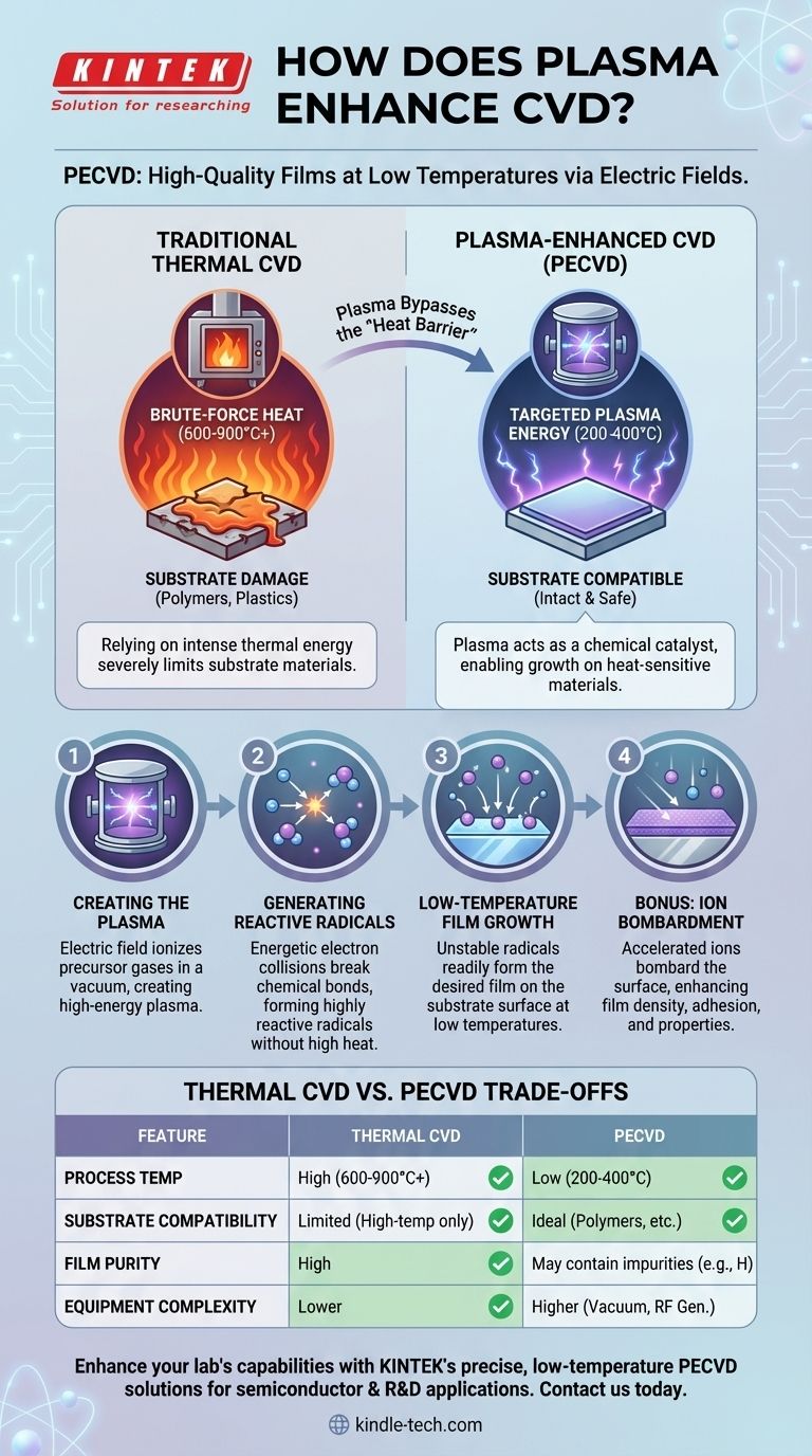
Plasma enhances Chemical Vapor Deposition (CVD) by using an electric field to generate highly reactive chemical species at low temperatures. This process, known as PECVD, bypasses the need for the intense heat required in traditional thermal CVD. By creating a plasma, the precursor gases are broken down into reactive ions and radicals that readily form a film on a substrate, enabling deposition on materials that cannot withstand high heat.
While traditional CVD relies on brute-force heat to initiate chemical reactions, Plasma-Enhanced CVD (PECVD) acts as a chemical catalyst. It uses the targeted energy of a plasma to do the "heavy lifting" of breaking down gases, enabling high-quality film growth at a fraction of the temperature.
The Core Problem: The High-Temperature Barrier of Thermal CVD
To understand the value of plasma, we must first recognize the fundamental limitation of conventional thermal CVD.
The Need for Brute-Force Heat
Traditional thermal CVD works by heating a substrate in the presence of precursor gases. The high temperature (often 600-900°C or higher) provides the raw thermal energy needed to break the chemical bonds within the gas molecules.
Substrate Limitations
This intense heat requirement severely restricts the types of materials that can be used as substrates. Many important materials, such as polymers, plastics, and complex semiconductor devices with pre-existing metal layers, would be damaged, melted, or destroyed at these temperatures.
How Plasma Solves the Temperature Problem
PECVD introduces a new energy source—an electric field—to drive the chemical reaction, fundamentally changing the process requirements.
Step 1: Creating the Plasma
The process begins by introducing precursor gases into a low-pressure vacuum chamber. An electric field, typically in the radio frequency (RF) range, is then applied across the chamber.
This field energizes the gas, stripping electrons from some of the gas molecules. The result is plasma: an ionized gas containing a mix of high-energy electrons, positive ions, and neutral chemical radicals.
Step 2: Generating Reactive Radicals Without Heat
This is the critical step. The high-energy electrons in the plasma collide with the stable precursor gas molecules. These collisions are energetic enough to fracture chemical bonds, creating a high concentration of chemically reactive radicals.
Crucially, this bond-breaking happens because of the energetic electron collisions, not because the gas itself is hot. The overall gas temperature remains low (typically 200-400°C).
Step 3: Low-Temperature Film Growth
These radicals are highly unstable and readily react with each other and the substrate surface to form the desired solid film. Because the radicals are already so reactive, they do not need high thermal energy from the substrate to complete the deposition process.
Step 4: The Bonus of Ion Bombardment
In addition to creating radicals, the plasma also produces ions. These ions are accelerated by the electric field and gently bombard the substrate surface. This low-energy bombardment can enhance film density, improve adhesion, and give engineers an additional parameter to control film properties like stress.
Understanding the Trade-offs
While powerful, PECVD is not a universal solution. It involves a distinct set of trade-offs compared to high-temperature methods.
Film Purity and Stress
Because the precursor gases are fragmented in a less controlled way than by pure thermal decomposition, PECVD films can sometimes incorporate unwanted elements, such as hydrogen from silane (SiH₄). Films can also exhibit higher internal stress compared to their high-temperature counterparts.
Equipment Complexity and Cost
A PECVD system is inherently more complex than a thermal CVD furnace. It requires a vacuum chamber, precise gas flow controllers, a high-power RF generator, and matching networks, which increases the initial investment and maintenance complexity.
Potential for Substrate Damage
While PECVD is prized for being low-temperature, the ion bombardment, if not properly controlled, can cause subtle damage to the substrate surface or the growing film. This is a critical parameter that must be optimized for sensitive electronic applications.
Making the Right Choice for Your Goal
The decision between thermal CVD and PECVD depends entirely on the requirements of your substrate and the desired film properties.
- If your primary focus is depositing on temperature-sensitive materials (like plastics, organics, or fully processed wafers): PECVD is the definitive and often only choice, as it prevents thermal damage.
- If your primary focus is achieving the highest possible film purity and crystalline quality (e.g., epitaxial silicon): High-temperature thermal CVD is often superior, as the clean, thermally driven reaction minimizes impurities.
- If your primary focus is high-throughput deposition of dielectric layers (like silicon nitride or oxide) in semiconductor manufacturing: PECVD provides an ideal balance of good film quality, high deposition rates, and compatibility with underlying device structures.
By understanding that plasma's role is to provide chemical energy without thermal energy, you can confidently select the deposition technique that best aligns with your material, cost, and performance goals.
Summary Table:
| Feature | Thermal CVD | Plasma-Enhanced CVD (PECVD) |
|---|---|---|
| Process Temperature | High (600-900°C+) | Low (200-400°C) |
| Substrate Compatibility | Limited to high-temp materials | Ideal for polymers, plastics, processed wafers |
| Primary Energy Source | Thermal energy | Electric field (plasma) |
| Film Purity | High | May contain impurities (e.g., hydrogen) |
| Equipment Complexity | Lower | Higher (vacuum, RF generator required) |
Ready to enhance your lab's capabilities with precise, low-temperature deposition? KINTEK specializes in advanced lab equipment and consumables, including PECVD systems tailored for semiconductor manufacturing, R&D, and materials science. Our solutions ensure high-quality film growth on temperature-sensitive substrates, boosting your research and production efficiency. Contact us today to discuss your specific needs and discover how KINTEK can support your laboratory goals!
Visual Guide
Related Products
- RF PECVD System Radio Frequency Plasma-Enhanced Chemical Vapor Deposition RF PECVD
- Inclined Rotary Plasma Enhanced Chemical Vapor Deposition PECVD Equipment Tube Furnace Machine
- Chemical Vapor Deposition CVD Equipment System Chamber Slide PECVD Tube Furnace with Liquid Gasifier PECVD Machine
- Inclined Rotary Plasma Enhanced Chemical Vapor Deposition PECVD Equipment Tube Furnace Machine
- Microwave Plasma Chemical Vapor Deposition MPCVD Machine System Reactor for Lab and Diamond Growth
People Also Ask
- What is an example of PECVD? RF-PECVD for High-Quality Thin Film Deposition
- What is plasma chemical vapor deposition? A Low-Temperature Thin Film Coating Solution
- How does Radio Frequency Enhanced Plasma Chemical Vapour Deposition (RF-PECVD) work? Learn the Core Principles
- What is the role of RF-PECVD in VFG preparation? Mastering Vertical Growth and Surface Functionality
- Why is a Matching Network Indispensable in RF-PECVD for Siloxane Films? Ensure Stable Plasma and Uniform Deposition


