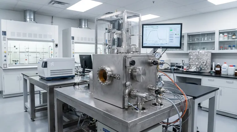
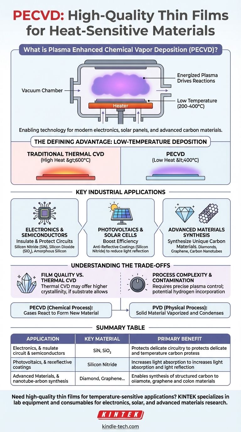
At its core, Plasma Enhanced Chemical Vapor Deposition (PECVD) is used to deposit high-quality thin films onto materials that cannot withstand high heat. This process is critical for manufacturing modern electronics, solar panels, and advanced carbon materials. Unlike traditional methods that rely solely on extreme temperatures, PECVD uses an energized plasma to drive the chemical reactions needed to form the film, enabling its use on delicate substrates.
While many deposition techniques exist, PECVD's defining feature is its ability to produce robust films at significantly lower temperatures. This single advantage unlocks a range of applications in electronics and photovoltaics that are impossible with high-temperature processes.
The Defining Advantage: Low-Temperature Deposition
The primary reason engineers and scientists choose PECVD is its ability to bypass the need for extreme heat. This is a fundamental departure from traditional Thermal Chemical Vapor Deposition (CVD).
How Plasma Replaces Heat
In traditional CVD, precursor gases must be heated to very high temperatures (often >600°C) to gain enough energy to react and form a solid film.
PECVD creates a plasma—an ionized gas—within the reaction chamber. This plasma energizes the precursor gases directly, allowing them to react and deposit onto a substrate at much lower temperatures, typically in the 200-400°C range.
Protecting Sensitive Substrates
This low-temperature capability is not just an efficiency gain; it is an enabling technology.
Many critical components, such as fully fabricated semiconductor wafers with existing metallic interconnects, flexible plastic substrates, or certain optical components, would be damaged or destroyed by the high temperatures of thermal CVD. PECVD allows for high-quality films to be deposited on these sensitive surfaces without causing harm.
Key Industrial Applications
The low-temperature advantage makes PECVD indispensable across several high-technology sectors.
Electronics and Semiconductor Manufacturing
PECVD is a workhorse in fabricating microelectronics. It is used to deposit dielectric films that insulate and protect the delicate circuitry on a chip.
Common materials include silicon nitride (SiN) for passivation (a final protective layer) and silicon dioxide (SiO₂) as an insulator between metal layers. It is also used to create amorphous silicon films, which are essential for the thin-film transistors (TFTs) that control pixels in flat-panel displays.
Photovoltaics and Solar Cells
In the solar industry, efficiency is everything. PECVD is used to apply silicon nitride anti-reflective coatings to the surface of silicon solar cells.
This thin film is engineered to reduce the amount of light that reflects off the cell's surface, allowing more photons to be absorbed and converted into electricity, thereby increasing the cell's overall efficiency.
Advanced Materials Synthesis
Specialized PECVD systems, particularly those using microwave plasma, are used at the cutting edge of materials science.
This technique is capable of synthesizing highly structured carbon materials with unique properties, including synthetic diamonds, graphene, and carbon nanotubes.
Understanding the Trade-offs
While powerful, PECVD is not a universal solution. Understanding its limitations is key to using it effectively.
Film Quality vs. Thermal CVD
Although PECVD films are high quality, films requiring the highest possible density, purity, and crystalline perfection are often still produced with high-temperature thermal CVD. The higher thermal energy can sometimes lead to a more ordered atomic structure, assuming the substrate can tolerate the heat.
Process Complexity and Contamination
Creating and maintaining a stable, uniform plasma is complex. Any instability can lead to non-uniform film thickness or properties.
Furthermore, the plasma process can incorporate other elements, like hydrogen, into the film, which can alter its electrical or optical characteristics. This must be carefully controlled.
Differentiating from PVD
It is important not to confuse PECVD with Physical Vapor Deposition (PVD). PECVD is a chemical process where gases react to form a new material on the substrate. PVD is a physical process where a solid source material is vaporized (e.g., via sputtering) and then condenses on the substrate without a chemical reaction.
Making the Right Choice for Your Goal
Selecting the correct deposition method requires matching the process capabilities to your primary objective.
- If your primary focus is coating heat-sensitive electronics or plastics: PECVD is the ideal choice due to its low-temperature processing capabilities.
- If your primary focus is maximizing solar cell efficiency: PECVD is the industry standard for depositing the silicon nitride anti-reflective coatings that boost performance.
- If your primary focus is achieving the absolute highest film crystallinity for a robust substrate: You may need to consider traditional high-temperature Thermal CVD, provided your substrate can withstand the heat.
- If your primary focus is depositing pure metals or alloys without a chemical reaction: Physical Vapor Deposition (PVD) is the more appropriate technology for your goal.
Ultimately, understanding the unique role of plasma is the key to leveraging PECVD for advanced, temperature-sensitive applications.
Summary Table:
| Application | Key Material Deposited | Primary Benefit |
|---|---|---|
| Electronics & Semiconductor | Silicon Nitride (SiN), Silicon Dioxide (SiO₂) | Protects and insulates delicate circuitry at low temperatures |
| Photovoltaics & Solar Cells | Silicon Nitride Anti-Reflective Coatings | Increases light absorption and solar cell efficiency |
| Advanced Materials Synthesis | Diamond, Graphene, Carbon Nanotubes | Enables synthesis of structured carbon materials |
Need high-quality thin films for your temperature-sensitive applications? KINTEK specializes in lab equipment and consumables, providing solutions for electronics, solar, and advanced materials research. Our expertise ensures you get the right PECVD technology to protect your substrates and enhance performance. Contact us today to discuss how we can support your laboratory needs!
Visual Guide
Related Products
- RF PECVD System Radio Frequency Plasma-Enhanced Chemical Vapor Deposition RF PECVD
- Inclined Rotary Plasma Enhanced Chemical Vapor Deposition PECVD Equipment Tube Furnace Machine
- Chemical Vapor Deposition CVD Equipment System Chamber Slide PECVD Tube Furnace with Liquid Gasifier PECVD Machine
- Inclined Rotary Plasma Enhanced Chemical Vapor Deposition PECVD Equipment Tube Furnace Machine
- Microwave Plasma Chemical Vapor Deposition MPCVD Machine System Reactor for Lab and Diamond Growth
People Also Ask
- What is an example of PECVD? RF-PECVD for High-Quality Thin Film Deposition
- What is plasma enhanced chemical vapour deposition process? Unlock Low-Temperature, High-Quality Thin Films
- How does plasma enhance CVD? Unlock Low-Temperature, High-Quality Film Deposition
- What is plasma chemical vapor deposition? A Low-Temperature Thin Film Coating Solution
- What is the role of RF-PECVD in VFG preparation? Mastering Vertical Growth and Surface Functionality


