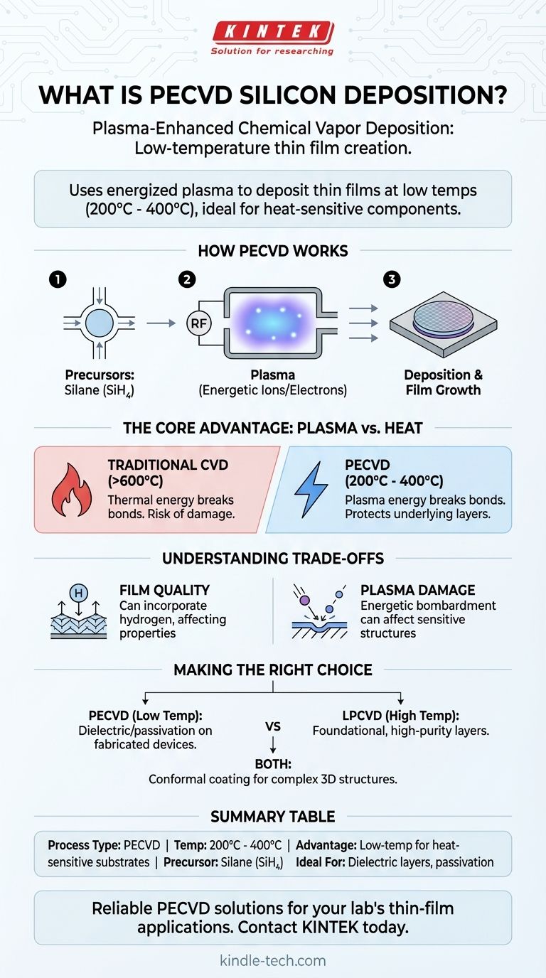
In short, PECVD silicon deposition is a process that uses an energized gas, known as plasma, to deposit a thin, uniform layer of silicon or a silicon compound onto a surface. Unlike purely heat-driven methods, the plasma provides the energy needed for the chemical reaction, allowing the deposition to occur at much lower temperatures. This makes it ideal for building complex devices with heat-sensitive components.
The core advantage of PECVD is its ability to create high-quality thin films at low temperatures. This capability is critical in modern electronics manufacturing, as it prevents damage to underlying layers or components that have already been fabricated on a substrate.
How PECVD Works: A Step-by-Step Breakdown
Plasma-Enhanced Chemical Vapor Deposition (PECVD) is a type of Chemical Vapor Deposition (CVD). The "chemical" part is key: the film is built from a chemical reaction, not by physically transferring material from a solid source.
The Role of Precursor Gases
The process begins by introducing specific gases, called precursors, into a vacuum chamber. For silicon-based films, a common precursor is silane (SiH₄).
Other gases are often added to create different materials, such as ammonia for silicon nitride (Si₃N₄) or nitrous oxide for silicon dioxide (SiO₂).
Generating the Plasma
An electric field, typically using a radio frequency (RF) source, is applied to the gas inside the chamber. This powerful field energizes the gas, stripping electrons from the precursor molecules and creating a plasma.
A plasma is a highly reactive state of matter containing a mix of ions, electrons, and neutral radicals.
The Chemical Reaction and Deposition
This is where the "plasma-enhanced" magic happens. The highly energetic particles within the plasma break apart the stable precursor gas molecules.
This creates chemically reactive fragments that are much more likely to bond to a surface. These fragments then land on the substrate (e.g., a silicon wafer), where they react and form a stable, solid thin film.
Why Plasma is the Critical Ingredient
The fundamental challenge in thin film deposition is providing enough energy to initiate a chemical reaction. PECVD's innovation lies in how it delivers that energy.
Replacing Heat with Plasma Energy
Traditional CVD methods rely on very high temperatures (often >600°C) to break down precursor gases. This thermal energy makes the molecules vibrate until their chemical bonds break.
PECVD uses the plasma's electrical energy to achieve the same result. The high-energy electrons in the plasma collide with gas molecules, breaking them apart directly. This allows for high-quality film deposition at much lower temperatures, typically between 200°C and 400°C.
The Low-Temperature Advantage
This lower processing temperature is the primary reason PECVD is so widely used. It allows for deposition on top of substrates that have already been processed and contain materials, like aluminum interconnects, that would be damaged or destroyed by high-temperature methods.
Understanding the Trade-offs
While powerful, PECVD is not a universal solution. The choice of deposition method always involves balancing cost, quality, and material compatibility.
Film Quality and Composition
Because PECVD runs at lower temperatures and uses hydrogen-containing precursors like silane, the resulting films often incorporate a significant amount of hydrogen. This can affect the film's electrical properties and density.
Films grown at higher temperatures, such as with Low-Pressure CVD (LPCVD), are typically purer and have higher density, which may be required for certain critical applications.
Potential for Plasma Damage
The same energetic plasma that drives the chemical reaction can also physically bombard the substrate surface. This can sometimes cause damage to highly sensitive electronic device structures.
Engineers must carefully tune the plasma conditions—such as pressure, power, and gas flow—to maximize the deposition rate while minimizing this potential damage.
Making the Right Choice for Your Goal
Selecting the right deposition technique depends entirely on the specific requirements of the film and the limitations of your substrate.
- If your primary focus is depositing a dielectric or passivation layer on a fully fabricated device: PECVD is almost always the correct choice due to its low-temperature process.
- If your primary focus is creating an extremely pure, dense, and uniform film for a foundational layer: A higher-temperature method like LPCVD might be superior, provided the substrate can tolerate the heat.
- If you need to coat a complex, 3D structure with a highly uniform film: PECVD or LPCVD are excellent choices due to their conformal coating capabilities, which are superior to line-of-sight physical methods.
Ultimately, PECVD enables the fabrication of the advanced, multi-layered microelectronic devices that power our modern world.
Summary Table:
| Feature | PECVD Silicon Deposition |
|---|---|
| Process Type | Chemical Vapor Deposition (CVD) enhanced by plasma |
| Typical Temperature | 200°C - 400°C |
| Key Advantage | High-quality films on heat-sensitive substrates |
| Common Precursor | Silane (SiH₄) |
| Ideal For | Dielectric layers, passivation on fabricated devices |
Need a reliable PECVD solution for your lab's thin-film applications? KINTEK specializes in lab equipment and consumables, serving laboratory needs. Our expertise ensures you get the right deposition tools to build complex, multi-layered devices without damaging heat-sensitive components. Contact our experts today to discuss how our PECVD systems can enhance your research and manufacturing processes!
Visual Guide
Related Products
- Chemical Vapor Deposition CVD Equipment System Chamber Slide PECVD Tube Furnace with Liquid Gasifier PECVD Machine
- RF PECVD System Radio Frequency Plasma-Enhanced Chemical Vapor Deposition RF PECVD
- Inclined Rotary Plasma Enhanced Chemical Vapor Deposition PECVD Equipment Tube Furnace Machine
- Inclined Rotary Plasma Enhanced Chemical Vapor Deposition PECVD Equipment Tube Furnace Machine
- 915MHz MPCVD Diamond Machine Microwave Plasma Chemical Vapor Deposition System Reactor
People Also Ask
- How expensive is chemical vapor deposition? Understanding the True Cost of High-Performance Coating
- What is plasma enhanced chemical vapor deposition PECVD equipment? A Guide to Low-Temperature Thin Film Deposition
- How are carbon nanotubes grown? Master Scalable Production with Chemical Vapor Deposition
- What types of substrates are used in CVD to facilitate graphene films? Optimize Graphene Growth with the Right Catalyst
- What are the processes of vapor phase deposition? Understand CVD vs. PVD for Superior Thin Films


