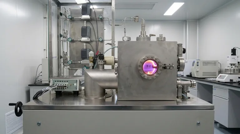
Plasma-Enhanced Chemical Vapor Deposition (PECVD) is a process used to create high-quality, thin-film coatings on a material's surface. Unlike traditional methods that rely solely on high heat, PECVD uses an energized gas, or plasma, to drive the necessary chemical reactions. This fundamental difference allows the process to run at much lower temperatures, making it a critical technology for coating heat-sensitive materials.
The essential advantage of PECVD is its ability to deposit durable, uniform films without the high temperatures that can damage delicate substrates. By using plasma to provide reaction energy instead of intense heat, it unlocks the ability to coat materials like plastics, integrated circuits, and flexible electronics.
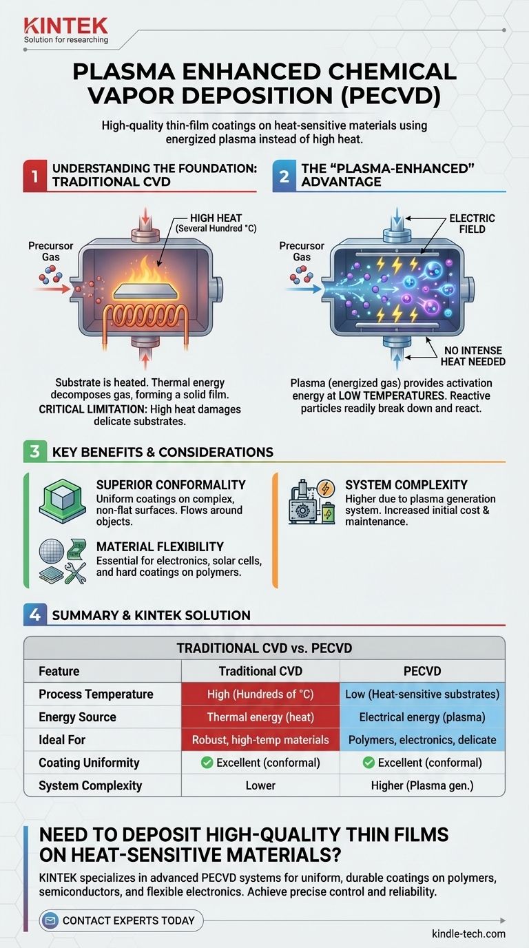
Understanding the Foundation: Traditional CVD
To grasp the innovation of PECVD, one must first understand the process it enhances: Chemical Vapor Deposition (CVD).
The Core Process
In a standard CVD process, a substrate (the object to be coated) is placed inside a vacuum chamber. A volatile precursor gas containing the elements of the desired coating is then introduced into the chamber.
How the Film Forms
The chamber and substrate are heated to a very high temperature. This thermal energy causes the precursor gas to decompose and react on the substrate's surface, forming a solid, thin film that bonds directly to the material.
The Primary Limitation: Heat
The critical requirement for traditional CVD is high heat, often several hundred degrees Celsius. This heat provides the "activation energy" needed to break the chemical bonds in the precursor gas. This limitation makes it impossible to coat materials with low melting points or those that would be damaged by thermal stress.
The "Plasma-Enhanced" Advantage
PECVD fundamentally changes the energy source for the reaction, moving from purely thermal energy to electrical energy.
Introducing Plasma
Instead of relying only on heat, PECVD applies an electric field to the precursor gas within the chamber. This energizes the gas, stripping electrons from atoms and creating a mixture of ions, electrons, and highly reactive neutral radicals. This energized state is plasma.
Energy Without Intense Heat
These reactive plasma particles are highly energetic and readily break down and react on the substrate's surface, even at much lower temperatures. The plasma provides the activation energy that heat would otherwise supply.
The Result: Broader Capabilities
By lowering the required process temperature, PECVD makes it possible to deposit high-quality films on a vast range of heat-sensitive substrates. This includes polymers, thin-film solar cells, and complex semiconductor devices that would be destroyed by traditional CVD temperatures.
Key Benefits and Considerations
PECVD is not simply a low-temperature alternative; it is part of a family of deposition methods with distinct characteristics.
Benefit: Superior Conformality
Like all CVD methods, PECVD excels at creating highly uniform coatings. Because the precursor is a gas, it flows around and coats all surfaces of a complex, three-dimensional object evenly, overcoming the "line-of-sight" limitations of other methods like Physical Vapor Deposition (PVD).
Benefit: Material Flexibility
The process is used to deposit a wide variety of films essential for modern technology. These include silicon nitride and silicon dioxide for electronics, anti-reflective coatings for solar cells, and hard, wear-resistant coatings for tools.
Consideration: System Complexity
Introducing a plasma generation system (which involves power supplies and electrodes) makes a PECVD reactor more complex than a simple thermal CVD system. This can impact initial equipment cost and maintenance requirements.
Making the Right Choice for Your Goal
Selecting the correct deposition method depends entirely on the substrate material and the desired outcome.
- If your primary focus is coating robust materials that can withstand high temperatures: Traditional thermal CVD can be a simpler and highly effective solution.
- If your primary focus is coating heat-sensitive substrates like polymers or fully fabricated electronic devices: PECVD is the definitive choice, as its low-temperature process prevents thermal damage.
- If your primary focus is achieving a perfectly uniform coating on complex, non-flat surfaces: Both CVD and PECVD offer a significant advantage over line-of-sight methods.
Ultimately, PECVD's use of plasma decouples reaction energy from high heat, dramatically expanding the frontier of advanced material deposition.
Summary Table:
| Feature | Traditional CVD | PECVD |
|---|---|---|
| Process Temperature | High (hundreds of °C) | Low (suitable for heat-sensitive substrates) |
| Energy Source | Thermal energy (heat) | Electrical energy (plasma) |
| Ideal For | Robust, high-temperature materials | Polymers, electronics, delicate substrates |
| Coating Uniformity | Excellent (conformal) | Excellent (conformal) |
| System Complexity | Lower | Higher (due to plasma generation) |
Need to deposit high-quality thin films on heat-sensitive materials? KINTEK specializes in advanced lab equipment, including PECVD systems, to help you achieve uniform, durable coatings for polymers, semiconductors, and flexible electronics. Our solutions ensure precise process control and reliability for your most demanding applications. Contact our experts today to discuss how we can enhance your laboratory capabilities!
Visual Guide
Related Products
- Inclined Rotary Plasma Enhanced Chemical Vapor Deposition PECVD Equipment Tube Furnace Machine
- Chemical Vapor Deposition CVD Equipment System Chamber Slide PECVD Tube Furnace with Liquid Gasifier PECVD Machine
- Inclined Rotary Plasma Enhanced Chemical Vapor Deposition PECVD Equipment Tube Furnace Machine
- RF PECVD System Radio Frequency Plasma-Enhanced Chemical Vapor Deposition RF PECVD
- Multi Heating Zones CVD Tube Furnace Machine Chemical Vapor Deposition Chamber System Equipment
People Also Ask
- Why is a PECVD system required for vertical graphene synthesis? Master Directional Control for 3D Nanostructures
- What is plasma enhanced chemical vapour deposition PECVD used for? Enable Low-Temp Thin Films for Electronics & Solar
- What are the advantages of plasma enhanced chemical vapor deposition? Enable Low-Temperature, High-Quality Film Deposition
- What are the benefits of plasma enhanced CVD? Achieve High-Quality, Low-Temperature Film Deposition
- What is plasma enhanced chemical vapor deposition PECVD equipment? A Guide to Low-Temperature Thin Film Deposition


